
Index 73
Precision rectifier circuit with integral circuit
Published:2012/9/23 21:14:00 Author:Ecco | Keyword: Precision rectifier , integral circuit
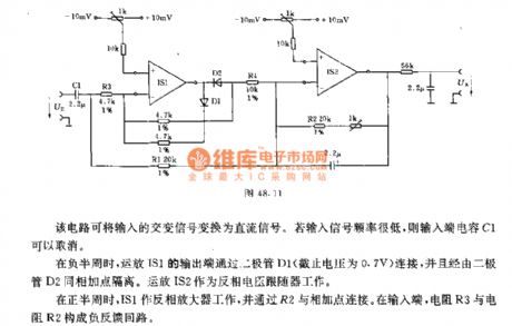
The circuit can switch input alternating signal to DC signal. If the input signal frequency is low, the input-terminal capacitor C1 can be canceled.In the negative half cycle, the output terminal of op amp IS1 is connected by diode D1 ( off voltage is 0.7V) and isolated from the same summing point via the diode D2. Op amp IS2 works as the inverting voltage follower.In the positive half cycle, IS1 works as an inverting amplifier and is connected to the summing point by R2. At the input terminal, the resistor R3 and resistor R2 constitute a negative feedback loop.
(View)
View full Circuit Diagram | Comments | Reading(985)
Broadband voltage follower circuit
Published:2012/9/23 21:30:00 Author:Ecco | Keyword: Broadband voltage follower
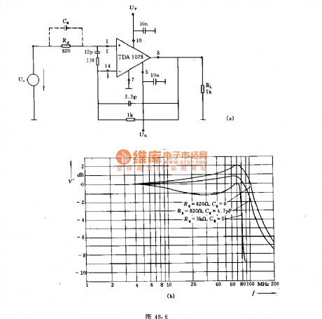
In the figure a, it is connected to frequency compensation circuit, and its amplification factor V '= 1, and it uses the full negative feedback. Small signal 3dB bandwidth frequency is 130MHz ( related to the load impedance ). If the load capacitance is large, it must be connected to resistor RD at the input end in series. Figure b shows the frequency characteristic curve of the voltage follower.
(View)
View full Circuit Diagram | Comments | Reading(696)
Dark activated relay circuit
Published:2012/9/21 2:34:00 Author:Ecco | Keyword: Dark activated relay
This Dark activated Switch can trigger a relay to operate an AC lamp at Sunset. The lamp remains on till morning and then turns off. This eliminates the need of switching the Porch lamp or Backyard lamp daily and also helps to light the premises of the house when the occupants are out of station.The circuit utilizes the light sensing property of LDR to activate the circuit. The LDR (Light Dependent Resistor) has very high resistance as high as 10 Meg ohms in dark which reduces to a few Ohms in bright light.
Variable resistor VR and the LDR forms a potential divider that gives a variable voltage to the inverting input (pin2) of IC1. The non inverting input (pin3) of IC1 gets a fixed voltage (half supply voltage) from the junction of the potential divider R1 and R2. Feedback Resistor R3 gives some hysteresis so that the relay turns on when the light level falls to a particular value and does not turns off again until the light level rises above this value. This prevents spurious switching by sensing mild changes in the light level. This also prevents relay clicking when the light level gradually falls at sunset.
During day time LDR gets sunlight and it conducts. This reduces the voltage at pin2 of IC1. Since this voltage level is lesser than the voltage at pin3, output of IC1 goes high to make the PNP transistor T1 off. Thus relay remains off during day time.
When the light level decreases at sunset, LDR cease to conduct and the voltage level at pin 2 increases above the voltage level at pin3.Output of IC1 then turns low and T1 conducts. This activates the relay and the AC load connected to the NO (Normally Open) contacts of the relay turns on. This condition remains until LDR illuminates in the morning and then the lamp turns off. Diode D1 protects T1 from back e.m.f when T1 switches off.
VR can be used to adjust the sensitivity of LDR at the particular light level, say at 6 pm to turns on the lamp.
Dark activated Relay Circuit diagram
IC uA 741 and Transistor BC 557 / 558
?
11 Responses to “Dark activated relay circuit”
source: electroschematics.com
(View)
View full Circuit Diagram | Comments | Reading(803)
Ultrasonic beam barrier circuit
Published:2012/9/21 2:33:00 Author:Ecco | Keyword: Ultrasonic , beam barrier
This circuit generates inaudible ultrasound to make a barrier across the entry. At the moment the circuit detects a break in the sound barrier, it generates a loud alarm indicating the entry of a person. This can be used to protects the entry passages and helps to detect unauthorized entry of persons in protected areas. The circuit has two sections. An Ultrasound transmitter and a receiver. Both the circuits use 40 kHz Ultrasound transmitter (TX) and ultrasound receiver (RX) pair to transmit and receive the ultrasound.
The Transmitter section uses the ultrasound transmitter TX in conjunction with an emitter coupled oscillator comprising T1 and T2, both BC 548. The values of resistors and capacitors determine the oscillation at 40 kHz frequency which exactly matches with that of the transmitter.
Ultrasound Transmitter
Ultrasound Receiver
The receiver section has a 40 kHz ultrasound receiver RX which is connected to the base of T1.It is a common emitter amplifier which amplifies the signals received by the RX. The amplified signal available from the collector of T1 is coupled via C2 to the signal detector stage comprising T2 ,D1 and C3. When RX continuously receives the ultrasound from TX, T3 remains saturated and conducts. This keeps T4 output conduction since its base is at ground potential. When the ultrasound beam breaks, T3 turns off and T4 conducts. The piezo buzzer connected to the collector of T4 sounds the alarm. Red LED indicates the standby mode showing that the alarm system is active.
Range of the circuit
Range is a few meters .Properly align TX and RX on the opposite sides of the entry ,so that alarm will be off if the RX receives ultrasound from TX.
40kHz Ultrasound transmitter receiver pair
?
2 Responses to “Ultrasonic beam barrier circuit”
source: electroschematics.com
(View)
View full Circuit Diagram | Comments | Reading(935)
27MHz CB receiver circuit
Published:2012/9/20 21:04:00 Author:Ecco | Keyword: 27MHz , CB receiver

This is a simple 27MHz FM-CB receiver circuit built with TCA440 for listening CB ( citizen’s band ) transmissions with FM (frequency modulation). The selection is made with ceramic filters. This 27 MHz receiver works with an intermediary frequency of 455 kHz. The input filter is 27 MF type, so we obtain an acceptable attenuation of the mirroring frequency.
CB 27MHz Receiver Circuit Schematic
Because the intermediary frequency filter is used without adapting transformer, the selection is at 40 dB. Because of the noise in the transmission pauses, the CB receiver circuit has a squelch circuit which reacts at 4.5 kHz domain noise.?
6 Responses to “27MHz CB receiver circuit”
Source: electroschematics.com
(View)
View full Circuit Diagram | Comments | Reading(3233)
DC Electronic Fuse
Published:2012/9/20 20:58:00 Author:Ecco | Keyword: DC Electronic Fuse


This DC electronic fuse never needs to be replaced. It can be repaired with just a single press of the start/reset button S1. Once S1 is pressed, the thyristor T1 triggers and the current flows to the consumer load through T1 and resistor RS. Even after releasing the start button, the current continue to flow as long as the current’s value does not sink below a certain level.
Electronic DC fuse circuit diagram
The current flowing through the thyristor T1 will sink below the holding level when the current is rerouted through the transistor T2 2N3055. T2 and RS are built into the electronic fuse circuit for this purpose. If the voltage drop at RS exceeds above base-emitter-diode trigger voltage of the T2, the transistor conducts thereby bypassing the thyristor. The resistance value of RS must be at least 0.2 W. It must be dimensioned that the product of RS multiplied by the fuse current value equals to 0.7 volts.
Once T2 bypasses the T1, the current flowing through the thyristor sinks below the holding level and the T1 shuts off. This in turn causes the voltage drop at resistor RS to sink below the base-emitter trigger voltage of T2 and the transistor shuts off. The end result is the shutting off of the whole circuit. The DC fuse can be reactivated by pressing the start/reset button.
The value of resistor R1 is dependent on the supply voltage. Multiply the supply voltage with 1 KW to get the value of R1. Connect the dc electronic fuse circuit to the PLUS line of the consumer load. THe coltage drop at the circuit is less than 1 volt.
DC fuse PCB layout
?
3 Responses to “DC Electronic Fuse”
(View)
View full Circuit Diagram | Comments | Reading(1429)
Operational amplifier offset adjustment method
Published:2012/9/20 1:13:00 Author:Ecco | Keyword: Operational amplifier, offset, adjustment method
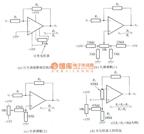
Figure a shows the adjustment when the circuit has offset.
Figure b shows the offset adjustment 1.
Figurec shows the offset adjustment 2.
Figure d shows the non inversion enlarged cases.
(View)
View full Circuit Diagram | Comments | Reading(945)
The modulator circuit for indicating low- voltage high - frequency signal
Published:2012/9/20 0:53:00 Author:Ecco | Keyword: modulator , indicating , low- voltage, high - frequency, signal
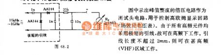
The peak rectified voltage doubler circuit shown in figure is used as a test head circuit for controlling the high ohmic display circuit (FET voltmeter). Because all high frequency components are very short leads, it can work at a high frequency. Lead length is not more than 2mm, and it may work in the high - frequency (VHF) region.
(View)
View full Circuit Diagram | Comments | Reading(576)
Active filter circuit with variable states
Published:2012/9/19 22:38:00 Author:Ecco | Keyword: Active filter , variable states

The circuit shown in figure has 2 outputs UA1 and UA2, the former is a high -pass filter output, and the latter is a band-pass filter output. The operational amplifiers A1 , A2 , A3 and A4 can use quad op amp OP-11FY or a LM124. Capacitor should use polystyrene film capacitor, and its accuracy should be less than ± 10%.
(View)
View full Circuit Diagram | Comments | Reading(1042)
High pass filter ( differentiator ) circuit
Published:2012/9/19 22:27:00 Author:Ecco | Keyword: High pass filter, differentiator

The circuit is the high-pass filter which is also used as pulse differentiator, output voltage is Ua and input voltage is Ue. Output voltage variation is about 12dB / octave. The value of the resistor R3 and R2 is equal.
(View)
View full Circuit Diagram | Comments | Reading(1011)
DC shunt motor commutation circuit
Published:2012/9/19 3:40:00 Author:Ecco | Keyword: DC shunt motor , commutation
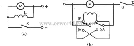
DC shunt motor's excitation coil and armature are connected in parallel, and it is shown in figure (a). If both the positive and negative poles are switching, it is impossible to change the direction of rotation of the motor. Therefore, it is the same with separately excited motor, you can change the direction of rotation by simply changing the armature or field coil wiring. Figure (b) shows a circuit which realize motor commutation by changing the exciting coil terminals.
(View)
View full Circuit Diagram | Comments | Reading(1038)
Motor winding heating and drying circuit with welding transformer
Published:2012/9/19 3:34:00 Author:Ecco | Keyword: Motor winding, heating , drying , welding transformer

For three - phase motor, the heating single phase power supply should be controlled about 110V, it can use a welding transformer to reduce the power supply voltage to 380V or 220V and access to the three-phase stator windings connected in series, and the circuit is shown in Fig. A stator winding current ( measured by the ammeter A ) is 70 % to 80% of the rated motor current, when it is energized 7 to 8 hours, the motor will be dried.
(View)
View full Circuit Diagram | Comments | Reading(2527)
Proximity switch circuit with TCA205A
Published:2012/9/19 1:58:00 Author:Ecco | Keyword: Proximity switch
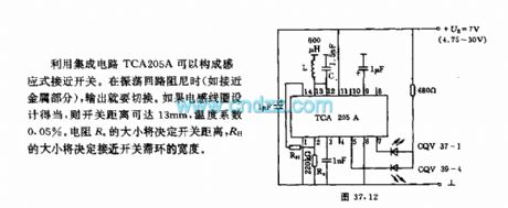
It uses integrated circuit TCA205A to form an inductive proximity switch. If the inductance coil is properly designed, the switching distance can be up to 13mm, the temperature coefficient is 0.05 % . The size of the resistor Ra will determine the switching distance, the RH will determine the width of the switch hysteresis loops.
(View)
View full Circuit Diagram | Comments | Reading(1924)
The magnetic circuit trip - voltage converter circuit with magnetic components
Published:2012/9/19 2:13:00 Author:Ecco | Keyword: magnetic circuit, trip - voltage converter , magnetic components
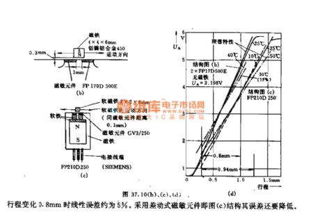
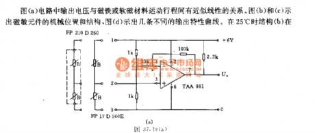
As shown in Figure a, it has a approximately linear relationship between the output voltage and the movement of the magnet or soft magnetic materials. Figures b and c illustrate the mechanical position and structure of the magneto-sensitive element, Figure d shows several different output characteristic curves. When temperature is at 25 ℃, the structure b changes 0.8mm, linearity error is about 5%. It uses differential magnetic components shown as Figure c to reduce structural error.
(View)
View full Circuit Diagram | Comments | Reading(613)
IR Beam breaker circuit
Published:2012/9/19 21:49:00 Author:Ecco | Keyword: IR Beam , breaker
This is an Infrared beam breaking alarm ideal to use in entry or passages.It is based on the working of the popular IR sensor Module TSOP 1738 which senses 38 kHz Infrared pulses from the IR LED of the transmitter. Range of the circuit is about 5 meters if the transmitter and receiver are properly aligned
TSOP 1738 IR sensor module responds to only 38kHz pulsed infrared rays. It will not sense continuous IR ray from the IR LED.So a transmitter circuit(as one in TV remote handset) based on 555 IC is required. Any standard transmitter circuit based on 555 IC can be used. But its output should be 38kHz exactly.TSOP 1738 gives 5 volt output and 5mA current in the off position. That is when IR rays are not available.Its output is current sinking so that when it receives 38kHz IR rays, output becomes zero.Pin 2 of the module should get a supply voltage between 4.5 to 6 volts.Higher voltage above 6 volts will destroy the device. The module is generally immune to ambient light, but may responds to sources of noice such as electronic ballasts.
IR Beam breaker Schematics
Out put from the IR module is given to the inverting input of IC1. LM311 is a precision voltage comparator . It looks like the common Op Amps like LM741, CA3130,CA 3140,TL071 etc.But its pin connections and output are different from other Op Amps.Pin 2 Non invertingPin3 InvertingPin 1 GroundPin8 VccPin7 Current sinking Output
The non inverting input of IC1 is connected to a potential divider comprising R1 and R2. When the IR sensor gets IR pulses from the transmitter, output of IC1 remains high. When the IR beam breaks, output from the sensor becomes high which triggers IC1. It then sinks current to activate buzzer and LED.
3 Responses to “IR Beam breaker circuit”
Source: electroschematic.com
(View)
View full Circuit Diagram | Comments | Reading(1189)
Wind Sound Effects circuit
Published:2012/9/19 21:43:00 Author:Ecco | Keyword: Wind Sound Effects

This wind sound effect generator circuit perfectly imitate the noise of the wind. Transistor T1 is connected as a Zener diode and will provide a noise signal to T2. The amplified signal by T2 is led to a frequency selective amplifier built with 741. With potentiometers P2a/P2b/P2c you can adjust the middle frequency of the filter and the wind sound. P1 adjusts the intensity of the sound which imitates the wind: an international scale Beaufort of wind intensity will make the adjustment easier.For P2 you may use a quadruple potentiometer of 15KΩ or 2 pots connected in parallel (P2c). If it is necessary the adjustment of the double T filter may be done for another value of P2. For that you need this formula:f = 1/2*pi*R*C with R=P2a=P2b=P2c and C=C5/2=C6=C7P2 may be simulated from many trimmer potentiometers (for vertical mounting of the plate).
Wind Effects Generator Circuit Schematic
?
One Response to “Wind Sound Effects circuit”
Source: electroschematic.com
(View)
View full Circuit Diagram | Comments | Reading(1007)
DIY Digital Thermometer Circuit
Published:2012/9/19 21:38:00 Author:Ecco | Keyword: DIY, Digital Thermometer

This diy digital thermometer circuit can measure temperatures up to 150°C with an accuracy of ±1°C. The temperature is read on a 1V full scale-deflection (FSD) moving-coil voltmeter or digital voltmeter.How the digital thermometer worksOperational amplifier IC 741 (IC3) provides a constant flow of current through the base-emitter junction of npn transistor BC108 (T1). The voltage across the base-emitter junction of the transistor is proportional to its temperature. The transistor used this way makes a low-cost sensor. You can use silicon diode instead of transistor.The small variation in voltage across the base-emitter junction is amplified by second operational amplifier (IC4), before the temperature is displayed on the meter. Preset VR1 is used to set the zero-reading on the meter and preset VR2 is used to set the range of temperature measurement.Operational amplifiers IC3 and IC4 operate off regulated ±5V power supply, which is derived from 3-terminal positive voltage regulator IC 7805 (IC1) and negative low-dropout regulator IC 7660 (IC2). The entire circuit works off a 9V battery.Assemble the circuit on a general-purpose PCB and enclose in a small plastic box. Calibrate the thermometer using presets VR1 and VR2. After calibration, keep the box in the vicinity of the object whose temperature isto be measured.
Sent by Mihail Dorutz, CH. Thanks a lot!
Digital Thermometer Circuit Schematic
5 Responses to “DIY Digital Thermometer Circuit”
Source: electroschematic.com
(View)
View full Circuit Diagram | Comments | Reading(1352)
Long Range IR Transmitter
Published:2012/9/19 21:23:00 Author:Ecco | Keyword: Long Range, IR Transmitter
This Long range Infrared transmitter can emit pulsed IR rays up to 10 meters. This IR transmitter is ideal to use in Infrared receivers using Phototransistor or Photodiode as IR sensor.The circuit is a simple Astable Multivibrator using IC NE555. Resistors R1, R2 and capacitor C1 fix the output frequency to 1 kHz. T1 is the Darlington high gain PNP transistor that drives two Infrared LEDs. Resistor R4 is the pull up resistor that keeps the base of T1 high for its proper working. By changing R2 with a 4.7K preset, output frequency can be changed. Red LED indicates whether the IR LED is working or not.
Long range IR Transmitter Circuit
?
4 Responses to “Long Range IR Transmitter”
Source: electroschematic.com
(View)
View full Circuit Diagram | Comments | Reading(1052)
DIY Tremolo Effect Circuit
Published:2012/9/19 21:21:00 Author:Ecco | Keyword: DIY , Tremolo Effect
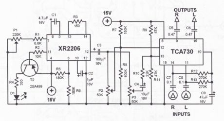
This tremolo effect circuit uses the XR2206 and the TCA730 IC which is designed as an electronic balance and volume regulator with frequency correction. The circuit is usefull for stereo channels and it also has the ability to simulate the Lesley effect aka rotating loudspeaker effect. How does the tremolo effect circuit works
Balance and volume settings are done with a linear potentiometer for both channels. If this potentiometer is replaced with an AC voltage source, a periodic modulation of the input signal can be achieved. This AC voltage source comes from the function generator IC XR2206. This IC generates square, triangle and sinewave signals but for this project we use only the sinewave.The modulation voltage can be varied with P1 from 1 Hz up to 25 Hz. Resistor R3 sets the operation level of the sinewave generator. R5 and R6 set the DC voltage and the sinewave amplitude at the output. C2 is a ripple filter. The squarewave output of the XR2206 drives T2 and a LED to optically display the frequency.The modulating voltage reaches pin 13 of TCA730 via P3 and R10. This input functions as the volume control or in this case the volume modulation. The degree of the balance modulation (Lesley effect) can be varied with P2. A regulated power supply using 7815 IC is recommended. Do not use a non-stabilized power supply since the current variations would influence the modulation negatively.Attach the 7815 IC to a good heatsink (about 10 cm2).
IC Tremolo effect circuit schematic
(View)
View full Circuit Diagram | Comments | Reading(1898)
Biofeedback by skin resistance
Published:2012/9/19 21:19:00 Author:Ecco | Keyword: Biofeedback , skin resistance
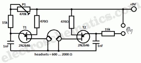
This simple circuit makes it possible for a particular type of biofeedback. The principle underlying the observation that a person’s skin resistance depends on the extent to which the person is relaxed; skin resistance increases with the depth of relaxation state.In the circuit shown, the skin resistance influence the oscillator frequency that is built with unijonction transistor T2. Both electrodes, which form a ring, are applied to two fingers of a hand. A speaker is used for hearing the sound whose height is a measure of the state of relaxation. The more profound state of relaxation is, the sound frequency is lower.
Relaxation monitor circuit schematic
The second oscillator, built with transistor T1, also produce a sound. In this case you can adjust the height of sound with potentiometer P1, at the frequency of the other oscillator, corresponding to the deepest state of relaxation. If the signals of the two systems are run separately in a stereo headset, the maximum relaxation is achieved when the right tone sounds at the same height at the left.
One Response to “Biofeedback by skin resistance”
Source: electroschematic.com
(View)
View full Circuit Diagram | Comments | Reading(948)
| Pages:73/471 At 206162636465666768697071727374757677787980Under 20 |
Circuit Categories
power supply circuit
Amplifier Circuit
Basic Circuit
LED and Light Circuit
Sensor Circuit
Signal Processing
Electrical Equipment Circuit
Control Circuit
Remote Control Circuit
A/D-D/A Converter Circuit
Audio Circuit
Measuring and Test Circuit
Communication Circuit
Computer-Related Circuit
555 Circuit
Automotive Circuit
Repairing Circuit