
Index 342
Auto counter for producivity 2
Published:2011/7/29 2:38:00 Author:Ecco | Keyword: Auto counter , producivity
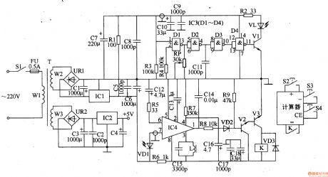
The auto counter for productivity described in the example uses infrared shading control circuit to accurately calculate the yield of the product.Itcan be used for beverages, beer and food packaging production line.
Power circuit is composed of the power switch Sl, fuse FU, power transformer T, rectifier bridge pile URl and UR2, three-terminal voltage regulator integrated circuit lCI and IC2, capacitors Cl-C8 and resistor R1.
Infrared transmitter circuit consists of NAND gate integrated circuit IC3 (Dl-D4), the transistor Vl, infrared light-emitting diode VL, resistors R2-R4, capacitors Cg-Cll and potentiometer RP.
Infrared receiver is composed of the infrared photodiode amplifier VDl, infrared signal processing integrated circuit IC4, resistors R5-R7, capacitors and inductors Cl2-Cl6 L. Control implementation circuit is composed of the resistors R8 and Rg, capacitors C17 and Cl8, diode VD2 and VD3, the transistor V2 and V3 and the relay K composition.
Count control circuit is composed of the fluorescent display calculators and thee normally open contact of K. (View)
View full Circuit Diagram | Comments | Reading(499)
VIDEO_MODULATOR_HOOKUP
Published:2009/6/23 5:06:00 Author:May

This circuit uses an ASTEC UM1683D,but it is typical of many RF video modulators used in VCRs and satellite receivers. (View)
View full Circuit Diagram | Comments | Reading(1672)
WINDOW_COMPARATOR
Published:2009/6/23 5:06:00 Author:May

IC1-c functions as a noninverting compara-tor, and IC1-a operates as an inverting compara-tor. Potentiometer RI and fixed resistors R2 and R3 form a divider chain that delivers slightly dif-ferent voltages to the two comparators. These voltages define the upper and lower limits of the circuit's switching window, which can be changed easily by varying R2 and R3. The LED glows only when the input voltage falls within the window region. (View)
View full Circuit Diagram | Comments | Reading(0)
LOW_POWER_dc_DOUBLER
Published:2009/6/23 5:02:00 Author:May

This dc voltage-doubler circuit based on the 555 can produce a dc output voltage equal to ap-proximately 2× the dc supply voltage. (View)
View full Circuit Diagram | Comments | Reading(1862)
LOW_POWER_dc_QUADRUPLER
Published:2009/6/23 5:01:00 Author:May

This dc voltage-quadrupler circuit based on the 555 can produce a dc output voltage equal to ap-proximately 4×the dc supply voltage. (View)
View full Circuit Diagram | Comments | Reading(2869)
PULSE_WIDTH_MODULATOR
Published:2009/6/23 5:00:00 Author:May

View full Circuit Diagram | Comments | Reading(1)
LOW_POWER_dc_TRIPLER
Published:2009/6/23 5:00:00 Author:May

This dc voltage-tripler circuit based on the 555 can produce proximately 3× the dc supply voltage. (View)
View full Circuit Diagram | Comments | Reading(4030)
FOUR_QUADRANT_MULTIPLIER_AS_DSB_MODULATOR
Published:2009/6/23 4:57:00 Author:May

View full Circuit Diagram | Comments | Reading(635)
DIGITAL_PULSE_WIDTH_MODULATION_CIRCUIT
Published:2009/6/23 4:54:00 Author:May

This circuit incorporates low-power Schottky transistor/tr ansistor-lo gic (TTL) devices in critical high-speed parts. The 5-MHz clock signal is converted to a 1-MHz signal by a 7490 decade counter configured to divide by 5. The 1-MHz signal is sent, via a clock synchronizer, to a three-stage binary divider that consists of three cascaded 74LS161 binary dividers. The synchronizer consists of a 74LS74 D flip-flop, a 7404 inverter gate, and a 7402 NOR gate. The dividers are programmed from the STD bus by means of three 7475 quad latches; this makes it possible to program the frequency divi-sion from 1 to 4096 (12 bits).The 1-MHz signal is also divided by 1000 by use of three cascaded 7490 decade counters, each configured to divide by 10; this provides a 1-kHz signal, which is sent to a 54121 monostable multivi-brator configured to provide a 0.1-ps pulse, bombarded with an ion beam source in preparation for the materials about to be deposited. While the surface is bombarded with an ion beam, an electron beam source is activated so that a layer of fused silica is vapor-deposited to a total desired thickness value (typically, 1 micron or t0,000 A). The layer offused silica serves as a surface stabilization layer for the next step.A metal mask with an aperture in the specified pattern of the sensor film is placed on the surface at the specified sensor location. The surface area exposed through the mask is cleaned by ion-beam bombardment for a predetermined time. Then as the bombardment continues, a metal (typically, nickel, platinum, and/or palladium) is vapor-deposited through the mask from the electron-beam source to form the sensor film. Deposition is continued until the thickness of the film reaches the value specified in the particular sensor design. A representative value for a nickel sensor film is 2500 A.Next, a pattern for thin film leads is defined by taping directly on the surface of the model with Kapton (or equivalent) polyimide tape. The thin film leads are fabricated by a combination of ion-beam bombardment and electron-beam vapor deposition like that used to deposit the sensor film.The metal vapor deposited in this step is typically copper, gold, or aluminum. A typical thickness for copper leads on the nickel sensor film is about 10,000 A. (View)
View full Circuit Diagram | Comments | Reading(2850)
Working principle circuit diagram of RS trigger
Published:2011/7/29 2:39:00 Author:Ecco | Keyword: Working principle , RS trigger
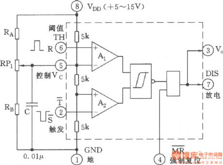
Figure shows the connection diagram,in which 555 is used as RS flip-flop. If removing the control voltage of control end of pin 5, adding a negative, positive control pulse to pin 2, pin 6 respectively, it will form a RS trigger circuit while 555 does not need any external components. R is the reset to control pin 6 of input terminal, also known as the threshold terminal (TH); S is the setting end to control pin 2 of input terminal, that is setting trigger T side. The interior of the output side (pin 3)is actually a push-pull output, so the low output is only 0.3V, high level closes to VDD, it has a strong load capacity; discharge end (pin 7) is the collector open (OC) or open-drain (OD) output. (View)
View full Circuit Diagram | Comments | Reading(1398)
32_CHANNEL_ANALOG_MULTIPLEXER
Published:2009/6/23 22:19:00 Author:Jessie
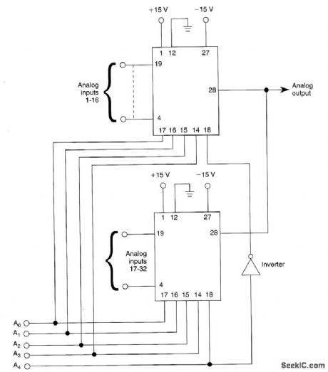
Using two Siliconix DG506 multiplexer chips, this 32-channel analog multiplexer selects 1 of 32 channels, depending on the data inputs A0 - A4. (View)
View full Circuit Diagram | Comments | Reading(1061)
SCM C8051FC40 and FM20L08 Expansion Circuits
Published:2011/7/26 2:05:00 Author:Michel | Keyword: SCM, Expansion Circuits


The monolithic integrated circuit expansion already has many mature examples and this paper will not list again and the above picture is monolithic conrolling FRAM principle circuit.The address signals multiplexing mode is used in the system, so they can produce ALE signal. FM20LO8 itself has latches and it chooses signal CE can not like SRAM and it needs precharging time and the signal produces HC04 and HC32.And the falling edge of address signals needs to lock and save and the expansion is shown as the above picture.
(View)
View full Circuit Diagram | Comments | Reading(586)
Low Voltage DC Power Charger Circuit
Published:2011/7/22 21:59:00 Author:Michel | Keyword: DC, Power Charge Circuit
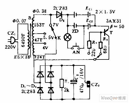
This circuit can be used as nickel cadmium and dry battery's charging and also used as genernal low voltage DC power. This circuit is composed of charging and DC output part.K2 is fast and slow charging choice switch.R2 and R3 are current limitting resistors which can alter charging current value.Usually, quick charging is controlled in 4 h or so, slow charging is about 14 h.NA,ZD consititute test circuit.Please install the batteries which will be charged before the charging.It's normal if the ZD has no light or has slight lihgt when AN is pressed.It's charged fully and can be used by electrical appliances if ZD has sparked for over 10S when the AN is pressed and chagring time meets the requirement. (View)
View full Circuit Diagram | Comments | Reading(439)
TWO_PHASE_RECTIFIER
Published:2009/6/23 4:21:00 Author:May

The waveform generated by the two-phase rectifier illustrates that the ripple is less than half that of a conventional single-phase circuit's wavefrom. Also,the ripple frequency is double that of the conventional circuit. The circuit amplitude changes in the ac input signal very rapidly,and it works equally will with current or voltage inputs. (View)
View full Circuit Diagram | Comments | Reading(678)
Motor vehicle steering flasher 2
Published:2011/7/29 3:05:00 Author:Ecco | Keyword: Motor vehicle , steering flasher
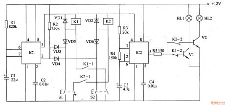
The motor vehicle steering flasher described in the example controls left and right turn signal by two control buttons respectively. Clicking the button will automatically turn on lights (one flash per second), it flashes about 20S then automatically turns off the power supply, thus avoiding the traffic accidents caused by forgetting to turn off lights.
The working principleThe motor vehicle steering flasher circuitis composed of monostable delay trigger, multivibrator and the trigger control circuit, it is shown as the chart 7-24.
Monostable circuitis composed of the time base trigger delay circuit ICl, resistors Rl, R2, capacitor Cl, C2.
Multivibrator integrated circuitis composed ofthe time base IC2, resistors R3, R4 and capacitors C3, C4.
Control circuit is composed of the control button Sl, S2, the relay Kl, K2, transistors Vl, V2 and diode VDl-VD6.
Component selection
Rl-R4 select the 1/4W metal film resistors or carbon film resistors; R5 selects the1W metal film resistor.
C uses the aluminium electrolytic capacitor with the voltage in 25V; C2 and C4 choose the monolithic capacitors or polyester capacitors.
Vl and V2 select 3DDl5 or DDO3 NPN silicon transistors. (View)
View full Circuit Diagram | Comments | Reading(497)
Battery Charging Circuit of MAX1737
Published:2011/7/23 2:13:00 Author:Michel | Keyword: Battery Charging Circuit

The above picture is battery charging circuit of MAX1737.There is PWM type synchronous rectifier step-down transformation circuit inside MAX1737.Its input voltage is 28 V and switch frequency is 300 kHZ. It has all funtions that charging circuit needs,namely,the input current monitoring, battery temperature monitoring, battery fault dindictaion, charging termination and the timing charging functions, etc.
MAX1737 tube feet functions are as follows.1 feet (VL)-The work power is input in DCIN port and this port is 5.4 V linear regulators output. Feet 2(ISETIN)-the input current limited port. (View)
View full Circuit Diagram | Comments | Reading(1868)
REGULATOR_CIRCUIT_FOR_BILATERAL_SOURCE_LOAD_POWER_SYSTEM
Published:2009/6/23 4:10:00 Author:May

The figure shows a circuit that regulates an output voltage, regardless of the direction of flow of output current. More specifically, it regulates the voltage at the left source or load, which can either supply power to or receive power from the right load or source, depending on the voltages and the direction of flow of current at the load/source terminals.The overall system can be characterized as a voltage-controlled current source with bilateral current capability. The current flowing between the two source/loads, averaged over a power-switching cycle, is made to depend on the pulse-width modulation that governs the operation of the two power-switching devices, and this pulse-width modulation is, in turn, a function of amplified currenterror and voltage-error signals. The voltage error is the difference between the actual output voltage and the output-reference voltage, which is the nominal output voltage at zero current. The pulsewidth modulation is varied to increase or decrease the current, as needed, to limit the excursion of output voltage from the reference value.An additional feature of this control circuit is that the maximum current in either direction can be limited by limiting the excursion of the output voltage from the zero-current value. Thus, external current-limiting circuitry is not necessary. (View)
View full Circuit Diagram | Comments | Reading(590)
VARACTORLESS_HF_MODULATOR
Published:2009/6/23 4:36:00 Author:May

Traditionally, high-frequency oscillators are frequency-modulated by using a varactor. However, varactors usually require a large voltage change to achieve a reasonable capacitance change-a prob-lem in many battery-powered systems.Such a problem can be overcome by employing base-charging capacitance modulation. Resistor RI establishes Q1's current, and R2 allows control of the collector bias current byVmod The trans-mission line (T1) in the negative resistance-type oscillator determines the frequency of oscillation. T1 is a high-quality, low-loss, ceramic coaxial shorted quarter-wave transmission line. Under proper terminal impedances, a negative resistance is seen at Q1's base. T1 reacts with this negative resis-tance to produce sustained oscillations.Frequency modulation is accomplished by changing Q1's collector bias current and thus chang-ing Q1's base-charging capacitance. This effect is seen at Q1's base and causes a frequency shift in the resonators quarter-wave node. (View)
View full Circuit Diagram | Comments | Reading(0)
POSITIVE_REGULATO_WITH_o_TO_70_V_OUTPUT
Published:2009/6/23 4:34:00 Author:May

The op amp has one input at ground and a reference current drawn from its summing junction. With this arrangement, the output voltage is proportional to setting resistor R2. A negative supply is used to operate the op amp within its common-mode range, providing zero output with sink current and power a low-voltage bandgap reference, D1. The current drawn from this supply is under 150 mA, except when sinking a load current. The output load capacitor, C2, is part of the op-amp frequency compensation. (View)
View full Circuit Diagram | Comments | Reading(0)
VIDEO_MASTER
Published:2009/6/23 3:58:00 Author:May

The video master consists of a series of converters that place all your video sources on unused UHF channels, which then combines them with normal TV channels (terrestrial or cable into one ca-ble). That one cable can then feed several TV sets for whole-house coverage. The desired video source is selected with the TV set's tuner. All of the TV's remote-control features are retained.A complete kit of parts is available from North Country Radio, P.O. Box 53, Wykagyl Station, New Rochelle, NY 10804-0053A. (View)
View full Circuit Diagram | Comments | Reading(0)
| Pages:342/471 At 20341342343344345346347348349350351352353354355356357358359360Under 20 |
Circuit Categories
power supply circuit
Amplifier Circuit
Basic Circuit
LED and Light Circuit
Sensor Circuit
Signal Processing
Electrical Equipment Circuit
Control Circuit
Remote Control Circuit
A/D-D/A Converter Circuit
Audio Circuit
Measuring and Test Circuit
Communication Circuit
Computer-Related Circuit
555 Circuit
Automotive Circuit
Repairing Circuit