UAA2033T/OM1033T, UAA2065T, UAA2067G Selling Leads, Datasheet
MFG:PHILIPS Package Cooled:N/A D/C:522

UAA2033T/OM1033T, UAA2065T, UAA2067G Datasheet download

Part Number: UAA2033T/OM1033T
MFG: PHILIPS
Package Cooled: N/A
D/C: 522


MFG:PHILIPS Package Cooled:N/A D/C:522
UAA2033T/OM1033T, UAA2065T, UAA2067G Datasheet download
MFG: PHILIPS
Package Cooled: N/A
D/C: 522

Want to post a buying lead? If you are not a member yet, please select the specific/related part number first and then fill the quantity and your contact details in the "Request for Quotation Form" on the left, and then click "Send RFQ".Your buying lead can then be posted, and the reliable suppliers will quote via our online message system or other channels soon.
TOP
PDF/DataSheet Download
Datasheet: UAA1016B
File Size: 348095 KB
Manufacturer: MOTOROLA [Motorola, Inc]
Download : Click here to Download
PDF/DataSheet Download
Datasheet: UAA1016B
File Size: 348095 KB
Manufacturer: MOTOROLA [Motorola, Inc]
Download : Click here to Download
PDF/DataSheet Download
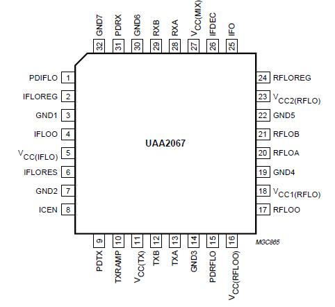
Datasheet: UAA2067G
File Size: 151771 KB
Manufacturer: PHILIPS [Philips Semiconductors]
Download : Click here to Download
The UAA2067G is a low-power transceiver intended for use in portable and base station transceivers complying with the DECT system. The IC performs in accordance with specifications in the -30 to +85°C temperature range.
The UAA2067G contains a front-end receiver for the 1800 to 1900 MHz frequency range, a high-frequency VCO for the 1650 to 1850 MHz range, a low-frequency VCO for the 100 to 140 MHz frequency range and a transmitter with a high-output power amplifier driver stage for the 1800 to 1900 MHz frequency range. Designed in an advanced BiCMOS process, it combines high performance with low-power consumption and a high degree of integration, thus reducing external component costs and total radio size.
Its first advantage is to provide typically 34 dB of image rejection in the receiver path. Thus, the image filter between the LNA and the mixer is redundant and consequently can be removed. The receive section consists of a low-noise amplifier that drives a quadrature mixer pair. Image rejection is achieved by this RF mixer pair and the two phase shifters in the I and Q channels that phase shift the IF by 45° and 135° respectively. The two phase shifted IFs are recombined and buffered to furnish the IF output signal.
Signals presented at the RF input at LO - IF frequency are rejected through this signal processing while signals at LO + IF frequency can form the IF signal.Its second advantage is to provide a good buffered high-frequency VCO signal to the RX and TX mixers and to the synthesizer-prescaler. Switching the receive or transmit section on gives a very small change in VCO frequency.
Its third advantage is to provide a good buffered low-frequency VCO signal to the TX mixers, to the synthesizer-prescaler and the second down conversion mixer in a double conversion receiver. Switching the transmit section on gives a very small change in VCO frequency.
The frequency of each VCO is determined by a resonator network that is external to the IC. Each VCO has a regulated power supply voltage that has been designed specifically for minimizing a change in frequency due to changes in the power supply voltage, which may be caused for instance by switching on the power amplifier.Its fourth advantage is to provide typically 33 dBc of image rejection in the single-sideband up-conversion mixer. Thus the image filter between the power amplifier and the antenna is redundant and may consequently be removed.
Image rejection is achieved in the internal architecture by two RF mixers in quadrature and two phase shifters in the low-frequency VCO signal that shifts the phase to 0° and 90°. The output signals of the mixers are summed to form the single-upper-sideband output signal.
The output stage is a high-level output buffer with an output power of approximately 4 dBm. The output level is sufficient to drive a three-stage bipolar preamplifier for DECT.
|
SYMBOL |
PARAMETER |
CONDITIONS |
MIN. |
MAX. |
UNIT |
| VCC | supply voltage |
- |
6 |
V | |
| GND | difference in ground supply voltage applied between all grounds | note 1 |
- |
+0.3 |
V |
| PI(max) | maximum power input |
- |
+20 |
dBm | |
| Tj(max) | maximum operating junction temperature |
- |
150 |
°C | |
| Pdis(max) | maximum power dissipation in stagnant air at 25°C |
- |
500 |
mW | |
| Tstg | storage temperature |
-65 |
+150 |
°C |
` Receiver with:
low noise amplifier
dual quadrature mixers for image rejection (lower sideband)
I and Q combining networks at a fixed IF
` Both high-frequency and low-frequency VCOs including buffers with good isolation for low pulling
` Transmitter with:
dual quadrature mixers for image rejection (lower sideband)
amplitude ramping circuit
amplifier with high output power.

Price: 4-6 USD
MT58L64L18CT-10 TQFP100

Price: 5-6.5 USD
DL-7140-211M laser tube

Price: 4-5 USD
74LVC74APG - IC FLIP FLOP D-Type POS-EDG DUAL 14TSSOP

Price: 6.5-8 USD
CYPRESS - Clock Synthesizer with Differential CPU Outputs

Price: 0.284-0.286 USD
PI5V330QEX Pericom Multiplexer Switch ICs

Price: 1-2 USD
IGBT power module, Single switch, 1200 V, Collector-emitter voltage, 430A

Price: 1-2 USD
a-Si TFT-LCD, NEC, 228.096Hmm, 560V

Price: 0.124-0.2 USD
PC354N1T - Mini-flat Package, AC Input Type Photocoupler - Sharp Electrionic Components

Price: 0.177-0.178 USD
RL1210JR51-XX-BL - Thick Film Chip Resistor Low Ohmic - TAITRON Components Incorporated

Price: 0.053-0.055 USD
STPS140A - POWER SCHOTTKY RECTIFIER - STMicroelectronics

Price: 1.45-1.5 USD
STA013 - MPEG 2.5 LAYER III AUDIO DECODER - STMicroelectronics

Price: 0.073-0.075 USD
SMBJ5347B - 5 Watt Surface Mount Silicon Zener Diodes - Micro Commercial Components
