Want to post a buying lead? If you are not a member yet, please select the specific/related part number first and then fill the quantity and your contact details in the "Request for Quotation Form" on the left, and then click "Send RFQ".Your buying lead can then be posted, and the reliable suppliers will quote via our online message system or other channels soon.
The main part of this circuit is a reference voltage source, which consists of a very stable, temperature-compensated band gap reference. An external capacitor (typ. 0.1 mF) must be connected to the voltage output Vref, to reduce the influence of fast transients in the supply voltage. The voltage at the SENSE input is divided by a resistor divider and compared with the reference voltage by a comparator. To achieve high accuracy, this divider is adjusted at wafer probe. When the input voltage is sensed to be lower than the threshold voltage, the thyristor is triggered, which discharges the timing capacitor C t . It is also possible to fire the thyristor via the RESIN input by a logic level (TTL level, active low). The thyristor is turned off again when either the voltage at the SENSE input (or RESIN input) increases beyond the threshold, or - during short supply voltage drops - the discharge current of the capacitor becomes lower than the hold current of the thyristor.
Thereafter, the capacitor is recharged by a current source 100 mA, the charge time being calculated as follows:
t C d t= 13 ×104×Ct Ct in F, t in s
The magnitude of charge current and therefore also the delay t d time is determined by the tolerance of the resistors in the integrated circuit. These tolerances, caused by the semiconductor manufacturing process, are not negligible. Therefore the delay time may vary -50 % to +100 %. However, for the applications discussed here this will not be a restriction. The diagram in figure 3 shows the typical delay time versus the capacitance of the external capacitor Ct.
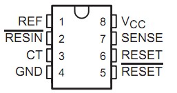
TL7709AC General Description
The TL77xxA family of integrated-circuit supply-voltage supervisors is specifically designed for use as reset controllers in microcomputer and microprocessor systems. The supply-voltage supervisor monitors the supply for undervoltage conditions at the SENSE input. During power up, the RESET output becomes active (low) when VCC attains a value approaching 3.6 V. At this point (assuming that SENSE is above VIT+), the delay timer function activates a time delay, after which outputs RESET and RESET go inactive (high and low, respectively). When an undervoltage condition occurs during normal operation, outputs RESET and RESET go active. To ensure that a complete reset occurs, the reset outputs remain active for a time delay after the voltage at the SENSE input exceeds the positive-going threshold value. The time delay is determined by the value of the external capacitor CT: td = 1.3 * 104 * CT, where CT is in farads (F) and td is in seconds (s).
During power down (assuming that SENSE is below VIT), the outputs remain active until the VCC falls below a maximum of 2 V. After this, the outputs are undefined.
An external capacitor (typically 0.1 µF for the TL77xxAC and TL77xxAI) must be connected to REF to reduce the influence of fast transients in the supply voltage.
The TL77xxAC series is characterized for operation from 0°C to 70°C. The TL77xxAI series is characterized for operation from 40°C to 85°C.
TL7709AC Maximum Ratings
Supply voltage, VCC (see Note 1) . . . . . . . . . . . . . . . . . . . . . . . . . . . .. . . . . . . . . . . . . . . . . 20 V Input voltage range, VI: RESIN . . . . . . . . . . . . . . . . . . . . . . . . . . . . . .. . . . . . .. . . 0.3 V to 20 V SENSE:TL7702A (see Note 2) . . . . . . . . . . . . . . . . . . . . 0.3 V to 20 V TL7705A. . . . . . . . . . . . . . . . . . . .. . . . . . . . . . .0.3 V to 20 V TL7709A. . . . . . . . . . . . . . . . . . . .. . . . . . . . . . .0.3 V to 20 V TL77012A, TL7715A. . . . . . . . . . .. . . . . . . . . . .0.3 V to 20 V High-level output current, IOH (RESET) . . . . . . . . . . . . . . . . . . . . . . . . . . . . . . . . . .. .. . .30 mA Low-level output current, IOL (RESET) . . . . . . . . . . . . . . .. . . . . . . . . . . . . . . . . .. .. . . . . .30 mA Package thermal impedance, JA (see Notes 2 and 3): D package . . . . . . . . . . . . . . . . .97°C/W P package . . . . . . . . . . . . . . . .127°C/W Case temperature for 60 seconds, TC: FK package . . . . . . . . . . . . . . .. . . . . . . . . . . . . . . 260°C Lead temperature 1,6 mm (1/16 inch) from case for 60 seconds: JG or U packages . . . . . 300°C Lead temperature 1,6 mm (1/16 inch) from case for 10 seconds: D or P packages . . . . .260°C Storage temperature range, Tstg. . . . . . . . . . . . . . . . . .. . . . . . . . . . . . . . . . . . 65°C to 150°C ? Stresses beyond those listed under "absolute maximum ratings" may cause permanent damage to the device. These are stress ratings only, and functional operation of the device at these or any other conditions beyond those indicated under "recommended operating conditions" is not implied. Exposure to absolute-maximum-rated conditions for extended periods may affect device reliability. NOTES: 1. All voltage values are with respect to the network ground terminal. 2. For proper operation of the TL7702A, the voltage applied to the SENSE terminal should not exceed VCC 1 V or 6 V, whichever is less. 3. Maximum power dissipation is a function of TJ(max), JA, and TA. The maximum allowable power dissipation at any allowable ambient temperature is PD = (TJ(max) TA)/JA. Operating at the absolute maximum TJ of 150°C can impact reliability. 4. The package thermal impedance is calculated in accordance with JESD 51, except for through-hole packages, which use a trace length of zero.