TL1454, TL145404, TL145406 Selling Leads, Datasheet
MFG:TI Package Cooled:07+ D/C:SMD

TL1454, TL145404, TL145406 Datasheet download

Part Number: TL1454
MFG: TI
Package Cooled: 07+
D/C: SMD


MFG:TI Package Cooled:07+ D/C:SMD
TL1454, TL145404, TL145406 Datasheet download
MFG: TI
Package Cooled: 07+
D/C: SMD

Want to post a buying lead? If you are not a member yet, please select the specific/related part number first and then fill the quantity and your contact details in the "Request for Quotation Form" on the left, and then click "Send RFQ".Your buying lead can then be posted, and the reliable suppliers will quote via our online message system or other channels soon.
TOP
PDF/DataSheet Download
Datasheet: TL1454
File Size: 400037 KB
Manufacturer: TI [Texas Instruments]
Download : Click here to Download
PDF/DataSheet Download
Datasheet: TL103W
File Size: 201561 KB
Manufacturer: TI [Texas Instruments]
Download : Click here to Download
PDF/DataSheet Download
Datasheet: TL145406
File Size: 169366 KB
Manufacturer: TI [Texas Instruments]
Download : Click here to Download
The TL1454 is a dual-channel pulse-width-modu-lation (PWM) control circuit, primarily intended for low-power, dc/dc converters. Applications include LCD displays, backlight inverters, notebook computers, and other products requiring small, high-frequency, dc/dc converters. Each PWM channel has its own error amplifier, PWM comparator, dead-time control comparator, and MOSFET driver. The voltage reference,oscillator, undervoltage lockout, and short-circuit protection are common to both channels.
Channel 1 is configured to drive n-channel MOSFETs in step-up or flyback converters, and channel 2 is configured to drive p-channel MOSFETs in step-down or inverting converters. The operating frequency is set with an external resistor and an external capacitor, and dead time is continuously adjustable from 0 to 100% duty cycle with a resistive divider network. Soft start can be implemented by adding a capacitor to the dead-time control (DTC) network. The error-amplifier common-mode input range includes ground, which allows the TL1454 to be used in ground-sensing battery chargers as well as voltage converters.
Supply voltage, VCC (see Note 1) . . . . . . . . . . . . . . . . . . . . . . . . . . . . . . . . . . . . . . . . . . . 23 V
Error amplifier input voltage: IN1+, IN1, IN2+, IN2 . . . . . . . . . . . . . . . . . . . . .. . . . . . . 23 V
Output voltage: OUT1, OUT2 . . . . . . . . . . . . . . . . . . . . . . . . . . . .. . . . . . . . . . . . . . . . . . . 20 V
Continuous output current: OUT1, OUT2 . . . . . . . . . . . . . . . . . . . . .. . . . . . . . . . . . . .±200 mA
Peak output current: OUT1, OUT2 . . . . . . . . . . . . . . . . . . . . . . .. . . . . . . . . . . . . . . . . . . . .1 A
Continuous total dissipation . . . . . . . . . . . . . . . . . . . . . . . . .. . .. See Dissipation Rating Table
Operating free-air temperature range, TA: C suffix . . . . . . . . . . . . . .. . . . . . . . 20°C to 85°C
I suffix . . . . . . . . . . . . . .. . . . . . . . 40°C to 85°C
Storage temperature range, Tstg . . . . . . . . . . . . . . . . . . . . . . . . . . . . . . . . . . 65°C to 150°C
Lead temperature 1,6 mm (1/16 inch) from case for 10 seconds . . . . . . . . . .. . . . . . . . 260°C
† Stresses beyond those listed under "absolute maximum ratings" may cause permanent damage to the device. These are stress ratings only, and functional operation of the device at these or any other conditions beyond those indicated under "recommended operating conditions" is not implied. Exposure to absolute-maximum-rated conditions for extended periods may affect device reliability.
NOTE 1: All voltage values are with respect to network GND.

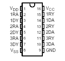
The TL145406 is a bipolar device containing three independent drivers and receivers that are used to interface data terminal equipment (DTE) with data circuit-terminating equipment (DCE). The drivers and receivers of the TL145406 are similar to those of the SN75188 quadruple driver and SN75189A quadruple receiver, respectively. The pinout matches the flow-through design of the SN75C1406 to reduce the board space required and to allow easy interconnection. The bipolar circuits and processing of the TL145406 provide a rugged low-cost solution for this function at the expense of quiescent power and external passive components relative to the SN75C1406.
The TL145406 complies with the requirements of TIA/EIA-232-F and ITU (formerly CCITT) V.28 standards. These standards are for data interchange between a host computer and peripheral at signaling rates up to 20 kbit/s. The switching speeds of the TL145406 are fast enough to support rates up to 120 kbit/s with lower capacitive loads (shorter cables). Interoperability at the higher signaling rates cannot be assured unless the designer has design control of the cable and of the interface circuits at both ends. For interoperability at signaling rates to 120 kbit/s, use of TIA/EIA-423-B (ITU V.10) and TIA/EIA-422-B (ITU V.11) standards is recommended. The TL145406 is characterized for operation from 0to 70.

Price: 4-6 USD
MT58L64L18CT-10 TQFP100

Price: 5-6.5 USD
DL-7140-211M laser tube

Price: 4-5 USD
74LVC74APG - IC FLIP FLOP D-Type POS-EDG DUAL 14TSSOP

Price: 6.5-8 USD
CYPRESS - Clock Synthesizer with Differential CPU Outputs

Price: 0.284-0.286 USD
PI5V330QEX Pericom Multiplexer Switch ICs

Price: 1-2 USD
IGBT power module, Single switch, 1200 V, Collector-emitter voltage, 430A

Price: 1-2 USD
a-Si TFT-LCD, NEC, 228.096Hmm, 560V

Price: 0.124-0.2 USD
PC354N1T - Mini-flat Package, AC Input Type Photocoupler - Sharp Electrionic Components

Price: 0.177-0.178 USD
RL1210JR51-XX-BL - Thick Film Chip Resistor Low Ohmic - TAITRON Components Incorporated

Price: 0.053-0.055 USD
STPS140A - POWER SCHOTTKY RECTIFIER - STMicroelectronics

Price: 1.45-1.5 USD
STA013 - MPEG 2.5 LAYER III AUDIO DECODER - STMicroelectronics

Price: 0.073-0.075 USD
SMBJ5347B - 5 Watt Surface Mount Silicon Zener Diodes - Micro Commercial Components
