STV7801-1A, STV7801-30, STV7801S Selling Leads, Datasheet
MFG:ST Package Cooled:DIP D/C:09+

STV7801-1A, STV7801-30, STV7801S Datasheet download

Part Number: STV7801-1A
MFG: ST
Package Cooled: DIP
D/C: 09+


MFG:ST Package Cooled:DIP D/C:09+
STV7801-1A, STV7801-30, STV7801S Datasheet download
MFG: ST
Package Cooled: DIP
D/C: 09+

Want to post a buying lead? If you are not a member yet, please select the specific/related part number first and then fill the quantity and your contact details in the "Request for Quotation Form" on the left, and then click "Send RFQ".Your buying lead can then be posted, and the reliable suppliers will quote via our online message system or other channels soon.
TOP
PDF/DataSheet Download
Datasheet: STV0020
File Size: 1497237 KB
Manufacturer:
Download : Click here to Download
PDF/DataSheet Download
Datasheet: STV0020
File Size: 1497237 KB
Manufacturer:
Download : Click here to Download
PDF/DataSheet Download
Datasheet: STV7801S
File Size: 145160 KB
Manufacturer: STMICROELECTRONICS [STMicroelectronics]
Download : Click here to Download
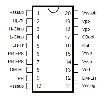
STV7801 is a monolithic integrated circuit implemented in STMicroelectronics BCD proprietary technology designed as a switched power supply generator for data drivers in a Plasma Display Panel (P.D.P.) application.
The high load drive capability of the STV7801 reduces the number of devices necessary to drive a complete PDP (4 to 6 devices for a 42" VGA 16/9 PDP monitor).
The STV7801 high current drive capability provides a high power recovery efficiency coefficient superior to 85% on constant capacitive load.To limit the number of external components, the device integrates level shifters driven with 5V CMOS compatible levels.
To increase the reliability of the system, the device integrates several protections such as output over-voltage, over-temperature, power-ON protection.
| Symbol | Parameter | Value | Unit |
| Vdd | Logic Supply Range | -0.3,+14 | V |
| Vpp | Driver Supply Range | -0.3 , + 100 | V |
| VIn | Logic Input Voltage Range | -0.3, Vdd+0.3 | |
| Ih-Out | Main Switch High Side Current | -5 | A |
| Il-Out | Main Switch Low Side Current | 5 | A |
| Ipr-Hi | Power Recovery Current (note1) | -7 | A |
| Ipr-Lo | Power Recovery current (note1) | 7 | A |
| VCBoot-Vout | Difference between Boot voltage and output voltage | 14 | V |
| Tjmax | Maximum Junction Temperature (note2) |
Internally protected |
|
| Top | Operating Temperature Range | -20, +70 | |
| Tstg | Storage Temperature Range | -50, +150 |
Note 1 Peak current as defined in Figure 1 on page 9
Note 2 These parameters are measured during ST's internal qualification which includes temperature characterization
on standard and corner batches of the process. These parameters are not tested on the parts.

Price: 4-6 USD
MT58L64L18CT-10 TQFP100

Price: 5-6.5 USD
DL-7140-211M laser tube

Price: 4-5 USD
74LVC74APG - IC FLIP FLOP D-Type POS-EDG DUAL 14TSSOP

Price: 6.5-8 USD
CYPRESS - Clock Synthesizer with Differential CPU Outputs

Price: 0.284-0.286 USD
PI5V330QEX Pericom Multiplexer Switch ICs

Price: 1-2 USD
IGBT power module, Single switch, 1200 V, Collector-emitter voltage, 430A

Price: 1-2 USD
a-Si TFT-LCD, NEC, 228.096Hmm, 560V

Price: 0.124-0.2 USD
PC354N1T - Mini-flat Package, AC Input Type Photocoupler - Sharp Electrionic Components

Price: 0.177-0.178 USD
RL1210JR51-XX-BL - Thick Film Chip Resistor Low Ohmic - TAITRON Components Incorporated

Price: 0.053-0.055 USD
STPS140A - POWER SCHOTTKY RECTIFIER - STMicroelectronics

Price: 1.45-1.5 USD
STA013 - MPEG 2.5 LAYER III AUDIO DECODER - STMicroelectronics

Price: 0.073-0.075 USD
SMBJ5347B - 5 Watt Surface Mount Silicon Zener Diodes - Micro Commercial Components
