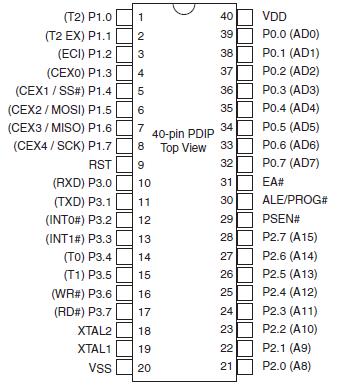
SST89E54RD, SST89E54RD2, SST89E54RD2-40-1--NJ Selling Leads, Datasheet
MFG:SST Package Cooled:05+ D/C:09+

SST89E54RD, SST89E54RD2, SST89E54RD2-40-1--NJ Datasheet download

Part Number: SST89E54RD
MFG: SST
Package Cooled: 05+
D/C: 09+


MFG:SST Package Cooled:05+ D/C:09+

SST89E54RD, SST89E54RD2, SST89E54RD2-40-1--NJ Datasheet download

MFG: SST
Package Cooled: 05+
D/C: 09+
Want to post a buying lead? If you are not a member yet, please select the specific/related part number first and then fill the quantity and your contact details in the "Request for Quotation Form" on the left, and then click "Send RFQ".Your buying lead can then be posted, and the reliable suppliers will quote via our online message system or other channels soon.
TOP
PDF/DataSheet Download
Datasheet: SST89E54RD2
File Size: 1008343 KB
Manufacturer: SST [Silicon Storage Technology, Inc]
Download : Click here to Download
PDF/DataSheet Download
Datasheet: SST89E54RD2
File Size: 1008343 KB
Manufacturer: SST [Silicon Storage Technology, Inc]
Download : Click here to Download
PDF/DataSheet Download
Datasheet: SST
File Size: 83114 KB
Manufacturer:
Download : Click here to Download
The SST89E5xRD2/RD and SST89V5xRD2/RD are embers of the FlashFlex51 family of 8-bit microcontroller roducts designed and manufactured with SST's patented nd proprietary SuperFlash CMOS semiconductor process echnology. The split-gate cell design and thick-oxide unneling injector offer significant cost and reliability benefits or SST's customers. The devices use the 8051 instruction et and are pin-for-pin compatible with standard 8051 icrocontroller devices.
The devices come with 16/24/40 KByte of on-chip flash EEPROM program memory which is partitioned into 2 independent program memory blocks. The primary Block 0 occupies 8/16/32 KByte of internal program memory space and the secondary Block 1 occupies 8 KByte of internal program memory space.
The 8-KByte secondary block can be mapped to the lowest location of the 8/16/32 KByte address space; it can also be hidden from the program counter and used as an independent EEPROM-like data memory.In addition to the 16/24/40 KByte of EEPROM program memory on-chip, the devices can address up to 64 KByte of external program memory. In addition to 1024 x8 bits of on-chip RAM, up to 64 KByte of external RAM can be addressed.
The flash memory blocks can be programmed via a standard 87C5x OTP EPROM programmer fitted with a special adapter and the firmware for SST's devices. During poweron reset, the devices can be configured as either a slave to an external host for source code storage or a master to an external host for an in-application programming (IAP) operation.The devices are designed to be programmed in-system and in-application on the printed circuit board for maximum flexibility. The devices are pre-programmed with an example of the bootstrap loader in the memory, demonstrating the initial user program code loading or subsequent user code updating via the IAP operation. The sample bootstrap loader is available for the user's reference and convenience only; SST does not guarantee its functionality or usefulness. Chip-Erase or Block-Erase operations will erase the pre-programmed sample code.

• 8-bit 8051-Compatible Microcontroller (MCU) with Embedded SuperFlash Memory
Fully Software Compatible
Development Toolset Compatible
Pin-For-Pin Package Compatible
• SST89E5xxRD2 Operation
0 to 40 MHz at 5V
• SST89V5xxRD2 Operation
0 to 33 MHz at 3V
• 1 KByte Internal RAM
• Dual Block SuperFlash EEPROM
8/16/32/64 KByte primary block + 8 KByte secondary block (128-Byte sector size for both blocks)
Individual Block Security Lock with SoftLock
Concurrent Operation during
In-Application Programming (IAP)
Memory Overlay for Interrupt Support during IAP
• Support External Address Range up to 64 KByte of Program and Data Memory
• Three High-Current Drive Ports (16 mA each)
• Three 16-bit Timers/Counters
• Full-Duplex, Enhanced UART
Framing Error Detection
Automatic Address Recognition
• Ten Interrupt Sources at 4 Priority Levels
Four External Interrupt Inputs
• Programmable Watchdog Timer (WDT)
• Programmable Counter Array (PCA)
• Four 8-bit I/O Ports (32 I/O Pins) and One 4-bit Port
• Second DPTR register
• Low EMI Mode (Inhibit ALE)
• SPI Serial Interface
• Standard 12 Clocks per cycle, the device has an option to double the speed to 6 clocks per cycle.
• TTL- and CMOS-Compatible Logic Levels
• Brown-out Detection
• Low Power Modes
Power-down Mode with External Interrupt Wake-up
Idle Mode
• Temperature Ranges:
Commercial (0°C to +70°C)
Industrial (-40°C to +85°C)
• Packages Available
44-lead PLCC
40-pin PDIP (Port 4 feature not available)
44-lead TQFP
