ML4621, ML4621CP, ML4621CQ Selling Leads, Datasheet
MFG:ML Package Cooled:DIP D/C:DIP

ML4621, ML4621CP, ML4621CQ Datasheet download

Part Number: ML4621
MFG: ML
Package Cooled: DIP
D/C: DIP


MFG:ML Package Cooled:DIP D/C:DIP
ML4621, ML4621CP, ML4621CQ Datasheet download
MFG: ML
Package Cooled: DIP
D/C: DIP

Want to post a buying lead? If you are not a member yet, please select the specific/related part number first and then fill the quantity and your contact details in the "Request for Quotation Form" on the left, and then click "Send RFQ".Your buying lead can then be posted, and the reliable suppliers will quote via our online message system or other channels soon.
TOP
PDF/DataSheet Download
Datasheet: ML4621
File Size: 165574 KB
Manufacturer: MICRO-LINEAR [Micro Linear Corporation]
Download : Click here to Download
PDF/DataSheet Download
Datasheet: ML4621CP
File Size: 165574 KB
Manufacturer: MICRO-LINEAR [Micro Linear Corporation]
Download : Click here to Download
PDF/DataSheet Download
Datasheet: ML4621CQ
File Size: 165574 KB
Manufacturer: MICRO-LINEAR [Micro Linear Corporation]
Download : Click here to Download
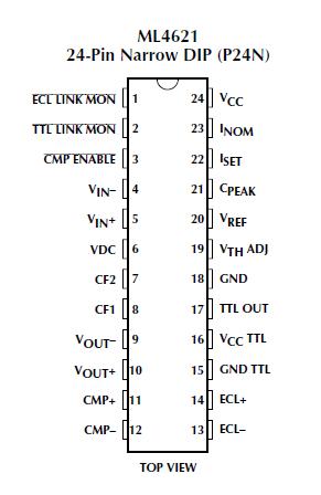
The ML4621 data quantizer is a low noise, wideband monolithic IC designed specifically for signal recovery applications in fiber-optic receiver systems. It contains a two stage wideband limiting amplifier which is capable of accepting an input signal as low as 2mV with a 55dB dynamic range. This high level of sensitivity is achieved by using a DC restoration feedback loop which nulls any offset voltage produced in the limiting amplifier. The output stage is a high speed comparator circuit with both TTL and ECL outputs. An enable pin is included for added control.
The minimum signal discriminator circuit provides a link monitor function with a user selectable reference voltage. This circuit monitors the peaks of the input signal and provides a logic level output indicating when the input falls below an acceptable level. This output can be used to disable the quantizer and/or drive an LED, providing a visible link status.
Absolute maximum ratings are those values beyond which the device could be permanently damaged. Absolute maximum ratings are stress ratings only and functional device operation is not implied.
VCC GND ................................................ 0.3V to 7.0V
VCC TTL GND TTL ................................... 0.3V to 7.0V
GND ............................................... 0.3V to VCC + 0.3V
Junction Temperature .............................................. 150°C
Storage Temperature Range ..................... 65°C to 150°C
Lead Temperature (Soldering, 10 sec) ..................... 260°C
Thermal Resistance (qJA)
24 Pin Narrow PDIP ......................................... 54°C/W
28 Pin PLCC ..................................................... 68°C/W

Price: 4-6 USD
MT58L64L18CT-10 TQFP100

Price: 5-6.5 USD
DL-7140-211M laser tube

Price: 4-5 USD
74LVC74APG - IC FLIP FLOP D-Type POS-EDG DUAL 14TSSOP

Price: 6.5-8 USD
CYPRESS - Clock Synthesizer with Differential CPU Outputs

Price: 0.284-0.286 USD
PI5V330QEX Pericom Multiplexer Switch ICs

Price: 1-2 USD
IGBT power module, Single switch, 1200 V, Collector-emitter voltage, 430A

Price: 1-2 USD
a-Si TFT-LCD, NEC, 228.096Hmm, 560V

Price: 0.124-0.2 USD
PC354N1T - Mini-flat Package, AC Input Type Photocoupler - Sharp Electrionic Components

Price: 0.177-0.178 USD
RL1210JR51-XX-BL - Thick Film Chip Resistor Low Ohmic - TAITRON Components Incorporated

Price: 0.053-0.055 USD
STPS140A - POWER SCHOTTKY RECTIFIER - STMicroelectronics

Price: 1.45-1.5 USD
STA013 - MPEG 2.5 LAYER III AUDIO DECODER - STMicroelectronics

Price: 0.073-0.075 USD
SMBJ5347B - 5 Watt Surface Mount Silicon Zener Diodes - Micro Commercial Components
