Want to post a buying lead? If you are not a member yet, please select the specific/related part number first and then fill the quantity and your contact details in the "Request for Quotation Form" on the left, and then click "Send RFQ".Your buying lead can then be posted, and the reliable suppliers will quote via our online message system or other channels soon.
The MDC5100 is designed to control GaAs RF switches which require positive and negative going control voltages to select the switch path. All input control signals are 3 V CMOSlogic compatible to allow for direct interface to a microcontroller. The device also has an accessory detect pin for use in applications where there is a portable handset to mobile adapter. The device is designed to interface directly with Double PullDouble Throw (DPDT) switches such as the M/ACom SW 363.
This device in combination with a GaAs RF switch can be used to achieve duplex isolation in many Time Division Duplex Radios like DECT or in Frequency Division Duplex Radios employing time division multiple access with staggered Transit/Receive time slots such as GSM. It can also be used to control an RF switch in dual band radio applications. The device is housed in a miniature Micro8 for minimum space utilization.
MDC5100 Maximum Ratings
Rating
Symbol
Value
Unit
Positive Supply Voltage
VCC
6
V
Negative Supply Voltage
|VEE|
12
V
Differential Supply Voltage
VCCVEE
15
V
Voltage Range at Any Input Pin (TxE, RxE, Acc)
Vin
1 to VCC
V
Junction Temperature
TJ
150
°C
Storage Temperature Range
Tstg
65 to +150
°C
MDC5100 Features
• Microminiature Low Profile Micro 8 Package • 3 V CMOS Logic Control Inputs • Ultralow Quiescent Current of 400 A Typical • Wide Operating Temperature Range of 40 to 85°C
MDC5100 Typical Application
• GSM and PCS Portable Phones • Mobile to Portable Accessories • Wireless LAN Modems • Specialized TDD and TDMA Radios • Dual Band Phones
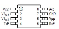
MDC5100 Connection Diagram
MDC5101 General Description
The MDC5101 inputs TxE and RxE Logic Signals with an accessory input termination option and, allows positive and negative control voltages in accordance with the enclosed truth table. This device is primarily intended to control GaAs RF switches. It is also designed to interface with most HCMOS MCUs such as the Motorola MC68338.
The MDC5101 is intended to replace a circuit of up to 18 discrete components and is available in a Micro8 package. This device, in combination with a compatible RF switch, can be used to achieve duplex isolation in any Time Division Duplex Radio like GSM and DCS1800 with staggered Transmit Receive Time Slots. It can also be used to control an RF switch in dual band radio applications.
This integrated solution in a Micro8 package compared with a discrete solution will add a great value in performance with less board space consumption.
MDC5101 Maximum Ratings
Rating
Symbol
Value
Unit
Positive Power Supply Voltage (1)
VCC
15
Vdc
Negative Power Supply Voltage (2)
VEE
12
Vdc
Differential Power Supply Voltage
VCCVEE
15
Vdc
Input Voltage (3)
Vin
VCC
Vdc
Output Current (4)
I1, I2
5.0
mAdc
Junction Temperature
TJ
150
°C
Operating Ambient Temperature Range
TA
40 to +85
°C
Storage Temperature Range
Tstg
65 to +150
°C
MDC5101 Features
• Miniature Micro8 Surface Mount Package Saves Board Space • Logic Level Control • Designed to Interface with Microcontrollers