MAX3770, MAX3770CEE., MAX3770CEET Selling Leads, Datasheet
MFG:N/A Package Cooled:04 D/C:216

MAX3770, MAX3770CEE., MAX3770CEET Datasheet download

Part Number: MAX3770
MFG: N/A
Package Cooled: 04
D/C: 216


MFG:N/A Package Cooled:04 D/C:216

MAX3770, MAX3770CEE., MAX3770CEET Datasheet download

MFG: N/A
Package Cooled: 04
D/C: 216
Want to post a buying lead? If you are not a member yet, please select the specific/related part number first and then fill the quantity and your contact details in the "Request for Quotation Form" on the left, and then click "Send RFQ".Your buying lead can then be posted, and the reliable suppliers will quote via our online message system or other channels soon.
TOP
PDF/DataSheet Download
Datasheet: MAX3770
File Size: 577711 KB
Manufacturer: MAXIM [Maxim Integrated Products]
Download : Click here to Download
PDF/DataSheet Download
Datasheet: MAX002
File Size: 42133 KB
Manufacturer: FILTRONIC [Filtronic Compound Semiconductors]
Download : Click here to Download
PDF/DataSheet Download
Datasheet: MAX002
File Size: 42133 KB
Manufacturer: FILTRONIC [Filtronic Compound Semiconductors]
Download : Click here to Download
The MAX3770 is a 2.125Gbps Fibre Channel repeater IC. The MAX3771 provides a pin-compatible solution for 1.063Gbps Fibre Channel. Both devices are optimized for use in Fibre Channel arbitrated-loop applications and operate from a 3.3V supply.
The MAX3770 is compatible with Fibre Channel jitter tolerance requirements and can recover data signals with up to 0.7 unit interval (UI) jitter. The circuit’s fully integrated phase-locked loop (PLL) provides a frequency lock indication and does not need an external reference clock.
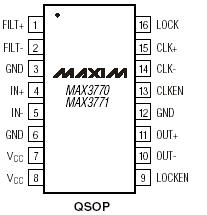
The MAX3770 provides low-jitter CML clock and data outputs. To reduce the external parts count, all signal inputs and outputs are internally terminated. The MAX3770/MAX3771 are available in 16-pin QSOP packages.
Supply Voltage, VCC..............................................-0.5V to +5.0V
Pin Voltage Levels (IN+, IN-, FILT+, FILT-,
LOCKEN, CLKEN, LOCK) .............................-0.5V to (VCC + 0.5V)
LOCK Output Current .........................................-1mA to +10mA
CML Output Currents OUT+, OUT-,
CLK+, CLK-........................................................-22mA to +22mA
Continuous Power Dissipation (TA = +70°C)
16-Pin TQFP (derate 6.7mW/°C above +70°C).............533mW
Operating Temperature Range............................0°C to +70°C
Storage Temperature Range .........................-55°C to +150°C
Processing Temperature (die) .......................................+400°C
Lead Temperature (soldering, 10s) ...............................+300°C
Stresses beyond those listed under “Absolute Maximum Ratings” may cause permanent damage to the device. These are stress ratings only, and functional operation of the device at these or any other conditions beyond those indicated in the operational sections of the specifications is not implied. Exposure to absolute maximum rating conditions for extended periods may affect device reliability.

