M52738P, M52739, M52739FP Selling Leads, Datasheet
MFG:MITSUBISHI Package Cooled:DIP28 D/C:98

M52738P, M52739, M52739FP Datasheet download

Part Number: M52738P
MFG: MITSUBISHI
Package Cooled: DIP28
D/C: 98


MFG:MITSUBISHI Package Cooled:DIP28 D/C:98
M52738P, M52739, M52739FP Datasheet download
MFG: MITSUBISHI
Package Cooled: DIP28
D/C: 98

Want to post a buying lead? If you are not a member yet, please select the specific/related part number first and then fill the quantity and your contact details in the "Request for Quotation Form" on the left, and then click "Send RFQ".Your buying lead can then be posted, and the reliable suppliers will quote via our online message system or other channels soon.
TOP
PDF/DataSheet Download
Datasheet: M52738P
File Size: 24595 KB
Manufacturer: MITSUBISHI [Mitsubishi Electric Semiconductor]
Download : Click here to Download
PDF/DataSheet Download
Datasheet: M52739FP
File Size: 207680 KB
Manufacturer: MITSUBISHI [Mitsubishi Electric Semiconductor]
Download : Click here to Download
PDF/DataSheet Download
Datasheet: M52739FP
File Size: 207680 KB
Manufacturer: MITSUBISHI [Mitsubishi Electric Semiconductor]
Download : Click here to Download
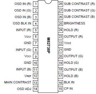
The M52737SP is a semiconductor integrated circuit amplifies video signals, having a 3-channel amplifier with a band width of 150MHz. The circuit also features the OSD mixing function.
The circuit is most useful with high-resolution displays that have OSD, and its function are available for each channel, including OSD blanking, OSD mixing, retrace blanking, wide-band amplification,contrast control (main and sub), and brightness control.
|
Symbol |
Psrameter |
Ratings |
Unit |
| Vcc | Supply voltage |
13.0 |
V |
| Pd | Power dissipation |
2403 |
mW |
| Topr | Ambient temperature |
-20to+85 |
°C |
| Tstg | Storage temperature |
-40to+150 |
°C |
| Vopr | Recommended supply voltage |
12.0 |
V |
| Vopr' | Recommended supply voltage range |
11.5to12.5 |
V |
| Surge | Electrostatic discharge |
±200 |
V |
• Frequency band width: RGB................................150MHz (3VP-P)
OSD..............................................50MHz
Input :RGB.............................................................0.7VP-P (typ.)
OSD...............................................3.0VP-P min. (positive)
BLK (for OSD)...............................3.0VP-P min. (positive)
Retrace BLK..................................3.0VP-P min. (positive)
Output :RGB...........................................................4.5VP-P (max.)
OSD...........................................................4.5VP-P (max.)
• To adjust contrast and OSD Adj, for each, two types of controls are provided, main and sub. With the main control, the contrast or OSD Adj of the 3-channels can be changed simultaneously. Sub controls are used to adjust the contrast of a given channel individually. The control terminals can be controlled by applying a voltage of 0 to 5V.
• The DC power remains stable at the IC output terminal because
a feedback circuit is built in.
|
Symbol |
Parameter |
Ratings |
Unit |
| Vcc | Supply voltage | 6.0 |
V |
| Pd | Power dissipation |
1700 |
mW |
| Topr | Ambient temperature |
-20to+85 |
|
| Tstg | Storage temperature |
-40to+150 |
|
| Vopr | Recommended supply |
5.0 |
V |
| Vopr' | voltage range |
4.7to5.3 |
V |
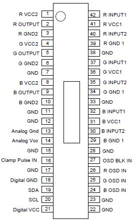
1.Frequency Band Width : RGB 180MHz(at -3dB)
OSD 80MHz
2.Input :RGB Input D range:Max1VP-P positive 2 input routes is changed by IIC BUS RGB OSD 3.5VP-P~5.0VP-P(positive)
3.Output :OSD BLK 3.5VP-P~5.0VP-P(positive) RGB 2.2VP-P (Max) OSD 2.0VP-P (Max)
4.Contrast :Output dynamic range 0.5~3.0V It can drive 14pF
5.Brightness :Both of sub and main contrast are controlled by IIC Bus(8bit).Control Range :-15dB~+15dB.
6.OSD Adjust :Both of sub and main contrast are controlled by IIC Bus(8bit).Control Range :0.5V~3.0V.
2 Control Ranges (Max1VP-P or Max2VP-P ) are able to be changed by IIC Bus.

Price: 4-6 USD
MT58L64L18CT-10 TQFP100

Price: 5-6.5 USD
DL-7140-211M laser tube

Price: 4-5 USD
74LVC74APG - IC FLIP FLOP D-Type POS-EDG DUAL 14TSSOP

Price: 6.5-8 USD
CYPRESS - Clock Synthesizer with Differential CPU Outputs

Price: 0.284-0.286 USD
PI5V330QEX Pericom Multiplexer Switch ICs

Price: 1-2 USD
IGBT power module, Single switch, 1200 V, Collector-emitter voltage, 430A

Price: 1-2 USD
a-Si TFT-LCD, NEC, 228.096Hmm, 560V

Price: 0.124-0.2 USD
PC354N1T - Mini-flat Package, AC Input Type Photocoupler - Sharp Electrionic Components

Price: 0.177-0.178 USD
RL1210JR51-XX-BL - Thick Film Chip Resistor Low Ohmic - TAITRON Components Incorporated

Price: 0.053-0.055 USD
STPS140A - POWER SCHOTTKY RECTIFIER - STMicroelectronics

Price: 1.45-1.5 USD
STA013 - MPEG 2.5 LAYER III AUDIO DECODER - STMicroelectronics

Price: 0.073-0.075 USD
SMBJ5347B - 5 Watt Surface Mount Silicon Zener Diodes - Micro Commercial Components
