LM5115MTCX+, LM5115MTCXNOPB, LM5116 Selling Leads, Datasheet
MFG:NSC Package Cooled:2007 D/C:2006

LM5115MTCX+, LM5115MTCXNOPB, LM5116 Datasheet download

Part Number: LM5115MTCX+
MFG: NSC
Package Cooled: 2007
D/C: 2006


MFG:NSC Package Cooled:2007 D/C:2006
LM5115MTCX+, LM5115MTCXNOPB, LM5116 Datasheet download
MFG: NSC
Package Cooled: 2007
D/C: 2006

Want to post a buying lead? If you are not a member yet, please select the specific/related part number first and then fill the quantity and your contact details in the "Request for Quotation Form" on the left, and then click "Send RFQ".Your buying lead can then be posted, and the reliable suppliers will quote via our online message system or other channels soon.
TOP
PDF/DataSheet Download
Datasheet: LM50
File Size: 180490 KB
Manufacturer: NSC [National Semiconductor]
Download : Click here to Download
PDF/DataSheet Download
Datasheet: LM50
File Size: 180490 KB
Manufacturer: NSC [National Semiconductor]
Download : Click here to Download
PDF/DataSheet Download
Datasheet: LM5116
File Size: 634564 KB
Manufacturer:
Download : Click here to Download
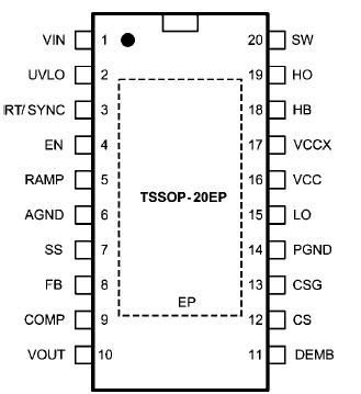
The LM5116 is a synchronous buck controller intended for step-down regulator applications from a high voltage or widely varying input supply. The control method is based upon current mode control utilizing an emulated current ramp. Current mode control provides inherent line feed-forward, cycle by cycle current limiting and ease of loop compensation. The use of an emulated control ramp reduces noise sensitivity of the pulse-width modulation circuit, allowing reliable control of very small duty cycles necessary in high input voltage applications.The operating frequency is programmable from 50kHz to 1MHz. The LM5116 drives external high-side and low-side NMOS power switches with adaptive dead-time control.A user-selectable diode emulation mode enables discontinuous mode operation for improved efficiency at light load conditions. A low quiescent current sleep mode disables the controller and consumes less than 10A of total input current. Additional features include a high voltage bias regulator, automatic switch-over to external bias for improved efficiency, thermal shutdown, frequency synchronization, cycle by cycle current limit and adjustable line under-voltage lockout. The device is available in a power enhanced TSSOP-20 package featuring an exposed die attach pad to aid thermal dissipation.
If Military/Aerospace specified devices are required,please contact the National Semiconductor Sales Office/Distributors for availability and specifications.
VIN to GND............................................. -0.3V to 100V
VCC, VCCX, UVLO to GND (Note 3)............. -0.3 to 16V
SW, CS to GND........................................ -3.0 to 100V
HB to SW ...................................................-0.3 to 16V
HO to SW........................................... -0.3 to HB+0.3V
VOUT to GND........................................... -0.3 to 100V
CSG to GND .................................................-1V to 1V
LO to GND ......................................-0.3 to VCC+0.3V
SS to GND.................................................. -0.3 to 7V
FB to GND ..................................................-0.3 to 7V
DEMB to GND ...........................................-0.3 to VCC
RT to GND ..................................................-0.3 to 7V
EN to GND .............................................-0.3 to 100V
ESD Rating HBM (Note 2) ...................................2 kV
Storage Temperature Range....... -55°C to +150°C
Junction Temperature .................................+150°C

Price: 4-6 USD
MT58L64L18CT-10 TQFP100

Price: 5-6.5 USD
DL-7140-211M laser tube

Price: 4-5 USD
74LVC74APG - IC FLIP FLOP D-Type POS-EDG DUAL 14TSSOP

Price: 6.5-8 USD
CYPRESS - Clock Synthesizer with Differential CPU Outputs

Price: 0.284-0.286 USD
PI5V330QEX Pericom Multiplexer Switch ICs

Price: 1-2 USD
IGBT power module, Single switch, 1200 V, Collector-emitter voltage, 430A

Price: 1-2 USD
a-Si TFT-LCD, NEC, 228.096Hmm, 560V

Price: 0.124-0.2 USD
PC354N1T - Mini-flat Package, AC Input Type Photocoupler - Sharp Electrionic Components

Price: 0.177-0.178 USD
RL1210JR51-XX-BL - Thick Film Chip Resistor Low Ohmic - TAITRON Components Incorporated

Price: 0.053-0.055 USD
STPS140A - POWER SCHOTTKY RECTIFIER - STMicroelectronics

Price: 1.45-1.5 USD
STA013 - MPEG 2.5 LAYER III AUDIO DECODER - STMicroelectronics

Price: 0.073-0.075 USD
SMBJ5347B - 5 Watt Surface Mount Silicon Zener Diodes - Micro Commercial Components
