Want to post a buying lead? If you are not a member yet, please select the specific/related part number first and then fill the quantity and your contact details in the "Request for Quotation Form" on the left, and then click "Send RFQ".Your buying lead can then be posted, and the reliable suppliers will quote via our online message system or other channels soon.
The DAC5675 is a 14-bit resolution high-speed digital-to-analog converter. The DAC5675 is designed for high-speed digital data transmission in wired and wireless communication systems, high-frequency direct-digital synthesis (DDS), and waveform reconstruction in test and measurement applications. The DAC5675 has excellent spurious free dynamic range (SFDR) at high intermediate frequencies, which makes the DAC5675 well suited for multicarrier transmission in TDMA and CDMA based cellular base transceiver stations BTS.
The DAC5675 operates from a single-supply voltage of 3.3 V. Power dissipation is 820 mW at fclk = 400 MSPS, fout = 70 MHz. The DAC5675 provides a nominal full-scale differential current output of 20 mA, supporting both single-ended and differential applications. The output current can be directly fed to the load with no additional external output buffer required. The output is referred to the analog supply voltage AVDD.
The DAC5675 is manufactured on Texas Instruments advanced high-speed mixed-signal BiCMOS process.
The DAC5675 comprises a LVDS (low-voltage differential signaling) interface. LVDS features a low differential voltage swing with a low constant power consumption across frequency, allowing for high speed data transmission with low noise levels, i.e., low electromagnetic interference (EMI). LVDS is typically implemented in low-voltage digital CMOS processes, making it the ideal technology for high-speed interfacing between the DAC5675 and high-speed low-voltage CMOS ASICs or FPGAs. The DAC5675 currentsource- array architecture supports update rates of up to 400 MSPS. On-chip edge-triggered input latches provide for minimum setup and hold times thereby relaxing interface timing.
DAC5675 Maximum Ratings
Supply voltage range: AVDD‡ . . . . . . . . . . . . . . . . . . . . . . . 0.3 V to 3.6 V DVDD§ . . . . . . . . . . . . . . . . . . . . . . . . 0.3 V to 3.6 V AVDD to DVDD . . . . . . . . . . . . . . . . . . 3.6 V to 3.6 V Voltage between AGND and DGND . . . . . . . . . . . . . . . . . . . 0.3 V to 0.5 V CLK, CLKC, SLEEP§ . . . . . . . . . . . . . . . . . . . . . . . . . 0.3 V to DVDD + 0.3 V Digital input D[13..0]A, D[13..0]B§ . . . . . . . . . . . . . 0.3 V to DVDD + 0.3 V IOUT1, IOUT2‡ . . . . . . . . . . . . . . . . . . . . . . . . . . . . 1.0 V to AVDD + 0.3 V EXTIO, BIASJ‡ . . . . . . . . . . . . . . . . . . . . . . . . . . . . . 0.3 V to AVDD + 0.3 V Peak input current (any input) . . . . . . . . . . . . . . . . . . . . . . . . . . . . . 20 mA Peak total input current (all inputs) . . . . . . . . . . . . . . . . . . . .. . . . . 30 mA Operating free-air temperature range, TA (DAC5675I) . . . . 40°C to 85°C Storage temperature range . . . . . . . . . . . . . . . . . . . . . . . . 65°C to 150°C Lead temperature 1,6 mm (1/16 inch) from the case for 10 seconds 260°C
DAC5675 Features
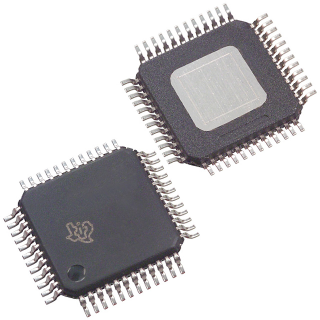
400-MSPS Update Rate LVDS-Compatible Input Interface Spurious Free Dynamic Range (SFDR) to Nyquist 69 dBc at 70-MHz IF, 400 MSPS W-CDMA Adjacent Channel Power Ratio ACPR 73 dBc at 30.72-MHz IF, 122.88 MSPS 71 dBc at 61.44-MHz IF, 245.76 MSPS Differential Scalable Current Outputs: 2 mA to 20 mA On-Chip 1.2-V Reference Single 3.3-V Supply Operation Power Dissipation: 820 at fclk = 400 MSPS, fout = 70 MHz Package: 48-Pin HTQFP PowerPad,TJA = 28.8°C/W
DAC5675 Typical Application
Cellular Base Transceiver Station Transmit Channel CDMA: WCDMA, CDMA2000, IS95 TDMA: GSM, IS136, EDGE/GPRS Supports Single-Carrier and Multicarrier Applications Test and Measurement: Arbitrary Waveform Generation Direct Digital Synthesis (DDS) Cable Modem Headend