BUK139-50L, BUK150-50DL, BUK1M200-50SDLD Selling Leads, Datasheet
MFG:NXP Package Cooled:2009+ROHS D/C:7200

BUK139-50L, BUK150-50DL, BUK1M200-50SDLD Datasheet download

Part Number: BUK139-50L
MFG: NXP
Package Cooled: 2009+ROHS
D/C: 7200


MFG:NXP Package Cooled:2009+ROHS D/C:7200
BUK139-50L, BUK150-50DL, BUK1M200-50SDLD Datasheet download
MFG: NXP
Package Cooled: 2009+ROHS
D/C: 7200

Want to post a buying lead? If you are not a member yet, please select the specific/related part number first and then fill the quantity and your contact details in the "Request for Quotation Form" on the left, and then click "Send RFQ".Your buying lead can then be posted, and the reliable suppliers will quote via our online message system or other channels soon.
TOP
PDF/DataSheet Download
Datasheet: BUK 456-800A
File Size: 63635 KB
Manufacturer:
Download : Click here to Download
PDF/DataSheet Download
Datasheet: BUK150-50DL
File Size: 42951 KB
Manufacturer: Philips
Download : Click here to Download
PDF/DataSheet Download
Datasheet: BUK1M200-50SDLD
File Size: 310114 KB
Manufacturer: PHILIPS [Philips Semiconductors]
Download : Click here to Download
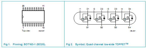
Monolithic temperature and overload protected logic level power MOSFET in TOPFET2 technology assembled in a 3 pin plastic package.
|
SYMBOL |
PARAMETER |
CONDITIONS |
MIN. |
MAX. |
UNIT |
|
VDS |
Continuous drain source voltage |
- |
- |
50 |
V |
|
ID |
Continuous drain current |
VIS = 5 V; Tmb = 25 °C |
- |
self -limited |
A |
|
ID |
Continuous drain current |
VIS = 5 V; Tmb 110 °C |
- |
20 |
A |
|
II |
Continuous input current |
- |
-5 |
5 |
mA |
|
IIRM |
Non-repetitive peak input current |
tp 1 ms |
-50 |
50 |
mA |
|
PD |
Total power dissipation |
Tmb 25 °C |
- |
90 |
W |
|
Tstg |
Storage temperature |
- |
-55 |
175 |
°C |
|
Tj |
Continuous junction temperature |
normal operation |
- |
150 |
°C |
|
Tsold |
Case temperature |
during soldering |
- |
260 |
°C |

| Symbol | Parameter | Conditions | Min | Max | Unit |
| VDS | drain-source voltage[1] |
- | 50 | V | |
| II | input current | clamping | - | 3 | mA |
| Ptot | tatal power dissipation[2] |
Tsp25; Figure 4 | - | 9.4 | W |
| IIMS | non-repetitive peak input current | tp1 ms | - | 10 | mA |
| Tstg | storage temperature | -55 | +150 | ||
| Tj | junction temperature[3] |
normal operation | - | 150 | |
| Overvoltage clamping[4] | |||||
| EDS(CL)S | non-repetitive drain-source clamping energy[5] | Tamb=25; IDMID(lim) (refer to Table 5); inductive load | - | 100 | mJ |
| EDS(CL)R | repetitive drain-source clamping[5] |
Tsp125;IDM=50mA;f=250Hz | - | 5 | mJ |
| Overload protection[6] | |||||
| VDS(prot) | protected drain-source voltage | VIS4V | - | 35 | V |
| Reverse diode | |||||
| IS | source(diode forward) current | Tsp25;VIS=0V | - | 2 | A |
| Electrostatic discharge | |||||
| Vesd | electrostatic discharge voltage | C=250 pF; R=1.5k | - | 2 | kV |
Power TrenchMOS
Overtemperature protection
Overload protection
Input-source voltage resets latched protection circuitry.
Inputusedtocontroloutputstageand supply overload protection circuits
5 V logic compatible input level
Current limiting
ESD protection for all pins
Overfatigue clamping for turn off of inductive loads
Low operating input current permits direct drive by micro-controller.

Price: 4-6 USD
MT58L64L18CT-10 TQFP100

Price: 5-6.5 USD
DL-7140-211M laser tube

Price: 4-5 USD
74LVC74APG - IC FLIP FLOP D-Type POS-EDG DUAL 14TSSOP

Price: 6.5-8 USD
CYPRESS - Clock Synthesizer with Differential CPU Outputs

Price: 0.284-0.286 USD
PI5V330QEX Pericom Multiplexer Switch ICs

Price: 1-2 USD
IGBT power module, Single switch, 1200 V, Collector-emitter voltage, 430A

Price: 1-2 USD
a-Si TFT-LCD, NEC, 228.096Hmm, 560V

Price: 0.124-0.2 USD
PC354N1T - Mini-flat Package, AC Input Type Photocoupler - Sharp Electrionic Components

Price: 0.177-0.178 USD
RL1210JR51-XX-BL - Thick Film Chip Resistor Low Ohmic - TAITRON Components Incorporated

Price: 0.053-0.055 USD
STPS140A - POWER SCHOTTKY RECTIFIER - STMicroelectronics

Price: 1.45-1.5 USD
STA013 - MPEG 2.5 LAYER III AUDIO DECODER - STMicroelectronics

Price: 0.073-0.075 USD
SMBJ5347B - 5 Watt Surface Mount Silicon Zener Diodes - Micro Commercial Components
