ADG719, ADG7198BRM, ADG7198RM Selling Leads, Datasheet
MFG:ADI Package Cooled:N/A D/C:09+

ADG719, ADG7198BRM, ADG7198RM Datasheet download

Part Number: ADG719
MFG: ADI
Package Cooled: N/A
D/C: 09+


MFG:ADI Package Cooled:N/A D/C:09+
ADG719, ADG7198BRM, ADG7198RM Datasheet download
MFG: ADI
Package Cooled: N/A
D/C: 09+

Want to post a buying lead? If you are not a member yet, please select the specific/related part number first and then fill the quantity and your contact details in the "Request for Quotation Form" on the left, and then click "Send RFQ".Your buying lead can then be posted, and the reliable suppliers will quote via our online message system or other channels soon.
TOP
PDF/DataSheet Download
Datasheet: ADG719
File Size: 509845 KB
Manufacturer: AD
Download : Click here to Download
PDF/DataSheet Download
Datasheet: ADG1204
File Size: 464641 KB
Manufacturer: AD [Analog Devices]
Download : Click here to Download
PDF/DataSheet Download
Datasheet: ADG1204
File Size: 464641 KB
Manufacturer: AD [Analog Devices]
Download : Click here to Download
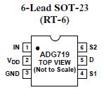
The ADG719 is a monolithic CMOS SPDT switch. This switch is designed on a submicron process that provides low power dissipation yet gives high switching speed, low on resistance and low leakage currents.
The ADG719 can operate from a single supply range of +1.8 V to +5.5 V, making it ideal for use in battery-powered instruments and with the new generation of DACs and ADCs from Analog Devices.
Each switch of the ADG719 conducts equally well in both directions when on. The ADG719 exhibits break-before-make switching action. Because of the advanced submicron process, 3 dB bandwidths of greater than 200 MHz can be achieved. The ADG719 is available in a 6-lead SOT-23 package and an 8-lead mSOIC package.
VDD to GND . . . . . . . . . . . . . . . . . . . . .. 0.3 V to +7 V
Analog, Digital Inputs2 . . . . . 0.3 V to VDD + 0.3 V or
30 mA, Whichever Occurs First
Peak Current, S or D . . . . . . . . . . . . . . . . . . . . .100 mA
(Pulsed at 1 ms, 10% Duty Cycle max)
Continuous Current, S or D . . . . . . . . . . . . . . . . .30 mA
Operating Temperature Range
Industrial (B Version) . . . . . . . . 40°C to +85°C
Storage Temperature Range . . . . . 65°C to +150°C
Junction Temperature . . . . . . . . . . . . . . . . . . . +150°C
mSOIC Package, Power Dissipation . . . . . . . . .315 mW
qJA Thermal Impedance . . . . . . . . . . . . . . 206°C/W
qJC Thermal Impedance . . . . . . . . . . . . . . 44°C/W
SOT-23 Package, Power Dissipation . . . . . . . 282 mW
qJA Thermal Impedance . . . . . . . . . . . . .229.6°C/W
qJC Thermal Impedance . . . . . . . . . . . . .91.99°C/W
Lead Temperature, Soldering
Vapor Phase (60 sec) . . . . . . . . . . . . . . . . . . . . . . . . +215°C
Infrared (15 sec) . . . . . . . . . . . . . . . . . . . . . . . . . . . . +220°C
ESD . . . . . . . . . . . . . . . . . . . . . . . . . . . . . . . . . . . . . . . . . . 1 kV
NOTES
1 Stresses above those listed under Absolute Maximum Ratings may cause permanent damage to the device. This is a stress rating only; functional operation of the device at these or any other conditions above those listed in the operational sections of this specification is not implied. Exposure to absolute maximum rating conditions for extended periods may affect device reliability. Only one absolute maximum rating may be applied at any one time.
2 Overvoltages at IN, S or D will be clamped by internal diodes. Current should be limited to the maximum ratings given.

Price: 4-6 USD
MT58L64L18CT-10 TQFP100

Price: 5-6.5 USD
DL-7140-211M laser tube

Price: 4-5 USD
74LVC74APG - IC FLIP FLOP D-Type POS-EDG DUAL 14TSSOP

Price: 6.5-8 USD
CYPRESS - Clock Synthesizer with Differential CPU Outputs

Price: 0.284-0.286 USD
PI5V330QEX Pericom Multiplexer Switch ICs

Price: 1-2 USD
IGBT power module, Single switch, 1200 V, Collector-emitter voltage, 430A

Price: 1-2 USD
a-Si TFT-LCD, NEC, 228.096Hmm, 560V

Price: 0.124-0.2 USD
PC354N1T - Mini-flat Package, AC Input Type Photocoupler - Sharp Electrionic Components

Price: 0.177-0.178 USD
RL1210JR51-XX-BL - Thick Film Chip Resistor Low Ohmic - TAITRON Components Incorporated

Price: 0.053-0.055 USD
STPS140A - POWER SCHOTTKY RECTIFIER - STMicroelectronics

Price: 1.45-1.5 USD
STA013 - MPEG 2.5 LAYER III AUDIO DECODER - STMicroelectronics

Price: 0.073-0.075 USD
SMBJ5347B - 5 Watt Surface Mount Silicon Zener Diodes - Micro Commercial Components
