Features: • SuperFAST HIGH DENSITY IN-SYSTEM PROGRAMMABLE LOGIC
- 8000 PLD Gates
- 96 I/O Pins, Nine Dedicated Inputs
- 192 Registers
- High Speed Global Interconnect
- Wide Input Gating for Fast Counters, State Machines, Address Decoders, etc.
- Small Logic Block Size for Random Logic
- Pinout Compatible with ispLSI 2096V and 2096VE
• 2.5V LOW VOLTAGE ARCHITECTURE
- Interfaces with Standard 3.3V Devices (Inputs and IOs are 3.3V Tolerant)
- 175 mA Typical Active Current
• HIGH PERFORMANCE E2CMOS® TECHNOLOGY
- fmax = 150 MHz Maximum Operating Frequency
- tpd = 6.0 ns Propagation Delay
- Electrically Erasable and Reprogrammable
- Non-Volatile
- 100% Tested at Time of Manufacture
- Unused Product Term Shutdown Saves Power IN-SYSTEM PROGRAMMABLE
- 2.5V In-System Programmability (ISP™) Using oundary Scan Test Access Port (TAP)
- Open-Drain Output Option for Flexible Bus Interface apability, Allowing Easy Implementation of Wired-OR Bus Arbitration Logic
- Increased Manufacturing Yields, Reduced Time-to-Market and Improved Product Quality
- Reprogram Soldered Devices for Faster Prototyping
• 100% IEEE 1149.1 BOUNDARY SCAN TESTABLE
• THE EASE OF USE AND FAST SYSTEM SPEED OF LDs WITH THE DENSITY AND FLEXIBILITY OF FPGAS
- Enhanced Pin Locking Capability
- Three Dedicated Clock Input Pins
- Synchronous and Asynchronous Clocks
- Programmable Output Slew Rate Control
- Flexible Pin Placement
- Optimized Global Routing Pool Provides Global nterconnectivity
• ispDesignEXPERT™ LOGIC COMPILER AND COMPLETE SP DEVICE DESIGN SYSTEMS FROM HDL YNTHESIS THROUGH IN-SYSTEM PROGRAMMING
- Superior Quality of Results
- Tightly Integrated with Leading CAE Vendor Tools
- Productivity Enhancing Timing Analyzer, Explore ools, Timing Simulator and ispANALYZER™
- PC and UNIX Platforms
Pinout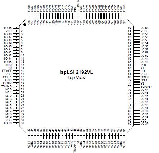 Specifications
Supply Voltage Vcc ................................ -0.5 to +4.05V
Input Voltage Applied ........................... -0.5 to +4.05V
Off-State Output Voltage Applied ......... -0.5 to +4.05V
Storage Temperature ............................ -65 to 150°C
Case Temp. with Power Applied ............ -55 to 125°C
Max. Junction Temp. (TJ) with Power Applied ... 150°C
1. Stresses above those listed under the "Absolute Maximum Ratings" may cause permanent damage to the device. Functional operation of the device at these or at any other conditions above those indicated in the operational sections of this specification is not implied (while programming, follow the programming specifications).
DescriptionThe ispLSI 2192VL is a High Density Programmable Logic Device containing 192 Registers, nine Dedicated Input pins, three Dedicated Clock Input pins, two dedicated Global OE input pins and a Global Routing Pool (GRP). The GRP provides complete interconnectivity between all of these elements. The ispLSI 2192VL features in-system programmability through the Boundary Scan Test Access Port (TAP) and is 100% IEEE 1149.1 Boundary Scan Testable. The ispLSI 2192VL offers nonvolatile reprogrammability of the logic, as well as the interconnect to provide truly reconfigurable systems.
The basic unit of logic on the ispLSI 2192VL device is the Generic Logic Block (GLB). The GLBs are labeled A0, A1 .. F7 (see Figure 1). There are a total of 48 GLBs in the ispLSI 2192VL device. Each GLB is made up of four macrocells. Each GLB has 18 inputs, a programmable AND/OR/Exclusive OR array, and four outputs which can be configured to be either combinatorial or registered. Inputs to the GLB come from the GRP and dedicated inputs. All of the GLB outputs are brought back into the GRP so that they can be connected to the inputs of any GLB on the device.

 ispLSI2192VL Data Sheet


