Features: * HIGH DENSITY PROGRAMMABLE LOGIC
- 8,000 PLD Gates
- 96 I/O Pins, Eight Dedicated Inputs
- 288 Registers
- High-Speed Global Interconnects
- Wide Input Gating for Fast Counters, State Machines, Address Decoders, etc.
- Small Logic Block Size for Random Logic
- Functionally Compatible with ispLSI 1048C and 104
* NEW FEATURES
- 100% IEEE 1149.1 Boundary Scan Testable
- ispJTAG(TM) In-System Programmable Via IEEE 114 (JTAG) Test Access Port
- User Selectable 3.3V or 5V I/O supports Mixed Voltage Systems (VCCIO Pin)
- Open Drain Output Option
* HIGH PERFORMANCE E2CMOS(R)TECHNOLOGY
- fmax = 170 MHz Maximum Operating Frequency
- tpd = 5.0 ns Propagation Delay
- TTL Compatible Inputs and Outputs
- Electrically Eraseable and Reprogrammable
- Non-Volatile
- 100% Tested at Time of Manufacture
* IN-SYSTEM PROGRAMMABLE
- Increased Manufacturing Yields, Reduced Time-to-Market and Improved Product Quality
- Reprogram Soldered Devices for Faster Prototypin
* OFFERS THE EASE OF USE AND FAST SYSTEM SPEED OF PLDs WITH THE DENSITY AND FLEXIBILI OF FIELD PROGRAMMABLE GATE ARRAYS
- Complete Programmable Device Can Combine Glu Logic and Structured Designs
- Enhanced Pin Locking Capability
- Four Dedicated Clock Input Pins
- Synchronous and Asynchronous Clocks
- Programmable Output Slew Rate Control to Minimize Switching Noise
- Flexible Pin Placement
- Optimized Global Routing Pool Provides Global Interconnectivity
* ispDesignEXPERT(TM) LOGIC COMPILER AND COM-PLETE ISP DEVICE DESIGN SYSTEMS FROM HDL SYNTHESIS THROUGH IN-SYSTEM PROGRAMMING
- Superior Quality of Results
- Tightly Integrated with Leading CAE Vendor Tools
- Productivity Enhancing Timing Analyzer, Explore Tools, Timing Simulator and ispANALYZER(TM)
- PC and UNIX PlatformsPinout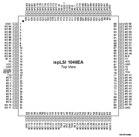
SpecificationsSupply Voltage Vcc. ................................. -0.5 to +7.0V
Input Voltage Applied........................-2.5 to VCC +1.0V
Off-State Output Voltage Applied .....-2.5 to VCC +1.0V
Storage Temperature.................................-65 to 150
Case Temp. with Power Applied ................-55 to 125
Max. Junction Temp. (TJ) with Power Applied ...... 150
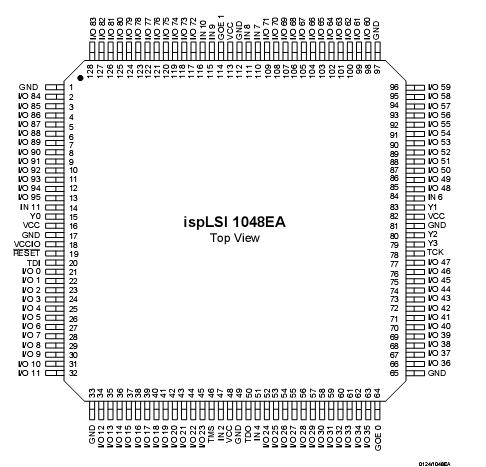
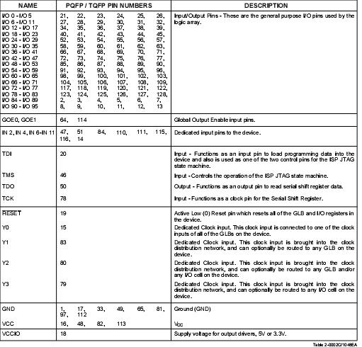
1. Stresses above those listed under the "Absolute Maximum Ratings" may cause permanent damage to the device. Functional operation of the device at these or at any other conditions above those indicated in the operational sections of this specification is not implied (while programming, follow the programming specifications).DescriptionThe ispLSI 1048EA is a High Density Programmable Logic Device containing 288 Registers, 96 Universal I/O pins, eight Dedicated Input pins, four Dedicated Clock Input pins, two dedicated Global OE input pins, and a Global Routing Pool (GRP). The GRP provides complete interconnectivity between all of these elements. The ispLSI 1048EA features 5V in-system programmability and in-system diagnostic capabilities via IEEE 1149.1
Test Access Port. The ispLSI 1048EA offers non-volatile reprogrammability of the logic, as well as the intercon-nect to provide truly reconfigurable systems. A functional superset of the ispLSI 1048 architecture, the ispLSI1048EA device adds user selectable 3.3V or 5V I/O and open-drain output options.
The basic unit of logic on the ispLSI 1048EA device is the Generic Logic Block (GLB). The GLBs are labeled A0,A1.F7 (see Figure 1). There are a total of 48 GLBs in the ispLSI 1048EA device. Each GLB has 18 inputs, a programmable AND/OR/Exclusive OR array, and four outputs which can be configured to be either combinato-rial or registered. Inputs to the GLB come from the GRP and dedicated inputs. All of the GLB outputs are brought
back into the GRP so that they can be connected to the inputs of any other GLB on the device.

 ispLSI1048EA Data Sheet


