Features: • HIGH-SPEED SWITCH MATRIX
- 7.5 ns Maximum Propagation Delay
- Typical Icc = 25 mA
- UltraMOS® Advanced CMOS Technology
• FLEXIBLE I/O MACROCELL
- Any I/O Pin Can be Input, Output, or Fixed
TTL High or Low
- Programmable Output Polarity
- Multiple Outputs Can be Driven by One Input
• IN-SYSTEM PROGRAMMABLE (5-VOLT ONLY)
- Programming Time of Less Than One Second
- 4-Wire Programming Interface
- Minimum 10,000 Program/Erase Cycles
• E2 CELL TECHNOLOGY
- Non-Volatile Reprogrammable Cells
- 100% Tested/100% Yields
- High Speed Electrical Erasure (<100ms)
- 20 Year Data Retention
• APPLICATIONS INCLUDE:
- Software-Driven Hardware Configuration
- Multiple DIP Switch Replacement
- Software Configuration of Add-In Boards
- Configurable Addressing of I/O Boards
- Multiple Clock Source Selection
- Cross-Matrix Switch
• ELECTRONIC SIGNATURE FOR IDENTIFICATIONPinout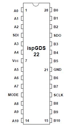 Specifications
Supply voltage VCC .................. .5 to +7V
Input voltage applied .............2.5 to VCC +1.0V
Off-state output voltage applied .......2.5 to VCC +1.0V
Storage Temperature............... 65 to 150°C
Ambient Temperature with
Power Applied .................. 55 to 125°C
1. Stresses above those listed under the "Absolute Maximum Ratings" may cause permanent damage to the device. These are stress only ratings and functional operation of the device at these or at any other conditions above those indicated in the operational sections of this specification is not implied (while programming, follow the programming specifications).
DescriptionThe Lattice Semiconductor ispGDS™ family is an ideal solution for reconfiguring system signal routing or replacing DIP switches used for feature selection. With today's demands for customer ease of use, there is a need for hardware which is easily reconfigured electronically without dismantling the system. The ispGDS devices address this challenge by replacing conventional switches with a software configurable solution. Since each I/O pin can be set to an ndependent logic level, the ispGDS devices can replace most DIP switch functions with about half the pin count, and without the need for additional pull-up resistors. In addition to DIP switch replacement, the ispGDS devices are useful as signal routing cross-matrix switches. This is the only non-volatile device on the market which can provide this flexibility.
With a maximum tpd of 7.5ns, and a typical active Icc of only 25 mA, these devices provide maximum performance at very low power levels. The ispGDS devices may be programmed in-system, using 5 volt only signals, through a simple 4-wire programming interface. The ispGDS devices are manufactured using
Lattice Semiconductor's advanced non-volatile E2CMOS process which combines CMOS with Electrically Erasable (E2) floating gate technology. High speed erase times (<100ms) allow the devices to be reprogrammed quickly and efficiently.
Each I/O macrocell can be configured as an input, an inverting or non-inverting output, or a fixed TTL high or low output. Any I/O pin can be driven by any other I/O pin in the opposite bank. A single input can drive one or more outputs in the opposite bank, allowing a signal (such as a clock) to be distributed to multiple destinations on the board, under software control. The I/Os accept and drive TTL voltage levels.
Unique test circuitry and reprogrammable cells allow complete AC, DC, and functional testing during manufacture. As a result, Lattice Semiconductor is able to deliver 100% field programmability and functionality of all Lattice Semiconductor products. In addition, 10,000 erase/write cycles and data retention in excess
of 20 years are specified.

 ispGDS22 Data Sheet


