Features: DSP Features:
• Dual data fetch
• Modulo and Bit-reversed modes
• Two 40-bit wide accumulators with optional saturation logic
• 17-bit x 17-bit single cycle hardware fractional/ integer multiplier
• All DSP instructins are single cycle
- Multiply-Accumulate (MAC) operation
• Single cycle ±16 shift
Peripheral Features:
• High current sink/source I/O pins: 25 mA/25 mA
• Up to five 16-bit timers/counters; optionally pair up 16-bit timers into 32-bit timer modules
• Up to four 16-bit Capture input functions
• Up to four 16-bit Compare/PWM output functions
• Data Converter Interface (DCI) supports common audio Codec protocols, including I2S and AC'97
• 3-wire SPI™ module (supports 4 Frame modes)
• I2C™ module supports Multi-Master/Slave mode and 7-bit/10-bit addressing
• Up to two addressable UART modules with FIFO buffers
• CAN bus module compliant with CAN 2.0B standard
Analog Features:
• 12-bit Analog-to-Digital Converter (A/D) with:
- 100 Ksps conversion rate
- Up to 13 input channels
- Conversion available during Sleep and Idle
• Programmable Low Voltage Detection (PLVD)
• Programmable Brown-out Detection and Reset generation
Special Microcontroller Features:
• Enhanced Flash program memory:
- 10,000 erase/write cycle (min.) for industrial temperature range, 100K (typical)
• Data EEPROM memory:
- 100,000 erase/write cycle (min.) for industrial temperature range, 1M (typical)
• Self-reprogrammable under software control
• Power-on Reset (POR), Power-up Timer (PWRT) and Oscillator Start-up Timer (OST)
• Flexible Watchdog Timer (WDT) with on-chip low power RC oscillator for reliable operation
• Fail-Safe Clock Monitor operation:
- Detects clock failure and switches to on-chip low power RC oscillator
Pinout
 Specifications
| Architecture |
16-bit |
| CPU Speed (MIPS) |
30 |
| Memory Type |
Flash |
| Program Memory (KB) |
48 |
| RAM Bytes |
2,048 |
| Temperature Range C |
-40 to 125 |
| Operating Voltage Range (V) |
2.5 to 5.5 |
| I/O Pins |
30 |
| Pin Count |
40 |
| System Management Features |
PBOR, LVD |
| Internal Oscillator |
7.37 MHz, 512 kHz |
| nanoWatt Features |
Fast Wake/Fast Control |
| Digital Communication Peripherals |
2-UART, 1-SPI, 1-I2C |
| Analog Peripherals |
1-A/D 13x12-bit @ 200(ksps) |
| Comparators |
0 |
| CAN (#, type) |
1 CAN |
| Capture/Compare/PWM Peripherals |
4/4 |
| Timers |
5 x 16-bit 2 x 32-bit |
| Parallel Port |
GPIO |
| Hardware RTCC |
No |
| DMA |
0 |
Absolute Maximum Ratings(†)
Ambient temperature under bias...................................................................-40°C to +125°C
Storage temperature ................................................................................... -65°C to +150°C
Voltage on any pin with respect to VSS (except VDD and MCLR) (Note 1)...-0.3V to (VDD + 0.3V)
Voltage on VDD with respect to VSS ..................................................................... -0.3V to +5.5V
Voltage onMCLR with respect to VSS ................................................................... 0V to +13.25V
Maximum current out of VSS pin .......................................................................................300 mA
Maximum current into VDD pin (Note 2)..............................................................................250 mA
Input clamp current, IIK (VI < 0 or VI > VDD) ....................................................................±20 mA
Output clamp current, IOK (VO < 0 or VO > VDD) ...............................................................±20 mA
Maximum output current sunk by any I/O pin........................................................................25 mA
Maximum output current sourced by any I/O pin ..................................................................25 mA
Maximum current sunk by all ports ......................................................................................200 mA
Maximum current sourced by all ports (Note 2)....................................................................200 mA
Note 1: Voltage spikes below Vss at the MCLR/Vpp pin, inducing currents greater than 80 mA, may cause latchup.
Thus, a series resistor of 50-100W should be used when applying a "low" level to the MCLR/Vpp pin, rather than pulling this pin directly to Vss.
2: Maximum allowable current is a function of device maximum power dissipation.
†NOTICE: Stresses above those listed under "Absolute Maximum Ratings" may cause permanent damage to the
device. This is a stress rating only and functional operation of the device at those or any other conditions above those
indicated in the operation listings of this specification is not implied. Exposure to maximum rating conditions for
extended periods may affect device reliability.
Note: All peripheral electrical characteristics are specified. For exact peripherals available on specific devices, please refer the the Family Cross Reference Table.
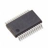
DescriptiondsPIC30F Motor Control 16-bit Digital Signal Controller.Seamless migration options from this device to dsPIC33F and PIC24 devices in similar packages.

 dsPIC30F4013 Data Sheet


