Features: ` 100 m, 4.5-A Peak MOSFET Switch for High Efficiency at 3-A Continuous Output Current
` Uses External Lowside MOSFET or Diode
` Output Voltage Adjustable Down to 0.891 V With 1% Accuracy
` Synchronizes to External Clock
` 180° Out of Phase Synchronization
` Wide PWM Frequency − Fixed 250 kHz, 500 kHz or Adjustable 250 kHz to 700 kHz
` Internal Slow Start
` Load Protected by Peak Current Limit and Thermal Shutdown
` Adjustable Undervoltage Lockout
` 16-Pin TSSOP PowerPADTM Package
Application· Industrial & Commercial Low Power Systems
· LCD Monitors and TVs
· Computer Peripherals
· Point of Load Regulation for High Performance DSPs, FPGAs, ASICs and Microprocessors
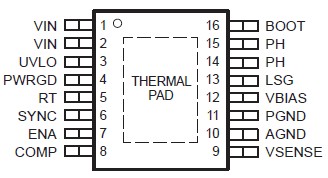
Pinout Specifications
|
UNIT |
| Input voltage range, VI |
VIN |
−0.3 V to 21.5 V |
| VSENSE |
−0.3 V to 8.0 V |
| UVLO |
−0.3 V to 8.0 V |
| SYNC |
−0.3 V to 4.0 V |
| ENA |
−0.3 V to 4.0 V |
| BOOT |
VI(PH) + 8.0 V |
| Output voltage range, VO |
VBIAS |
−0.3 to 8.5 V |
| LSG |
−0.3 to 8.5 V |
| SYNC |
−0.3 to 4.0 V |
| RT |
−0.3 to 4.0 V |
| PWRGD |
−0.3 to 6.0 V |
| COMP |
−0.3 to 4.0 V |
| PH |
−1.5 V to 22 V |
| Source current, IO |
PH |
Internally Limited (A) |
| LSG (Steady State Current) |
10 mA |
| COMP, VBIAS |
3 mA |
| Sink current, IS |
SYNC |
5 mA |
| LSG (Steady State Current) |
100 mA |
| PH (Steady State Current) |
500 mA |
| COMP |
3 mA |
| ENA, PWRGD |
10 mA |
| Voltage differential |
AGND to PGND |
±0.3 V |
| Operating virtual junction temperature range, TJ |
−40 to +150 |
| Storage temperature, Tstg |
−65 to +150 |
| Lead temperature 1,6 mm (1/16 inch) from case for 10 seconds |
260 |
(1) Stresses beyond those listed under "absolute maximum ratings" may cause permanent damage to the device. These are stress ratings only, and functional operation of the device at these or any other conditions beyond those indicated under "recommended operating conditions" is notimplied. Exposure to absolute-maximum-rated conditions for extended periods may affect device reliability.
DescriptionThe TPS54350 has the following features including Uses External Lowside MOSFET or Diode;Output Voltage Adjustable Down to 0.891 V With 1% Accuracy;Synchronizes to External Clock;Wide PWM Frequency - Fixed 250 kHz,500 kHz or Adjustable 250 kHz to 700 kHz;Internal Slow Start;Load Protected by Peak Current Limit and Thermal Shutdown;Adjustable Undervoltage Lockout;16-Pin TSSOP PowerPAD Package.
The TPS54350 is a medium output current synchronous buck PWM converter with an integrated high side MOSFET and a gate driver for an optional low side external MOSFET. Features include a high performance voltage error amplifier that enables maximum performance under transient conditions and flexibility in choosing the output filter inductors and capacitors. The TPS54350 has an under-voltage-lockout circuit to prevent start-up until the input voltage reaches 4.5 V; an internal slow-start circuit to limit in-rush currents; and a power good output to indicate valid output conditions. The synchronization feature is configurable as either an input or an output for easy 180° out of phase synchronization.The TPS54350 device is available in a thermally enhanced 16-pin TSSOP (PWP) PowerPAD(TM) package.TI provides evaluation modules and the SWIFT(TM) Designer software tool to aid in quickly achieving high-performance power supply designs to meet aggressive equipment development cycles.Please be aware that an important notice concerning availability, standard warranty, and use in critical applications of Texas Instruments semiconductor products and disclaimers thereto appears at the end of this data sheet.
Stresses beyond those listed under "absolute maximum ratings" may cause permanent damage to the device. These are stress ratings only, and functional operation of the TPS54350 at these or any other conditions beyond those indicated under "recommended operating conditions" is not implied. Exposure to absolute-maximum-rated conditions for extended periods may affect TPS54350 reliability.Adaptive dead time control prevents shoot through current from flowing in the integrated high-side MOSFET and the external low-side MOSFET TPS54350 during the switching transitions by actively controlling the turn on times of the drivers. The high-side driver does not turn on until the voltage at the gate of the low-side MOSFET is below 1 V.The low-side driver does not turn on until the voltage at the gate of the high-side MOSFET is below 1 V.

 TPS54350 Data Sheet


