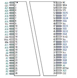
Features: • x8/x16 organization
• One hundred twenty-eight 128KB erase blocks
(128Mb)
Sixty-four 128KB erase blocks (64Mb)
Thirty-two 128KB erase blocks (32Mb)
• VCC, VCCQ, and VPEN voltages:
2.7V to 3.6V VCC operation
2.7V to 3.6V or 4.5V to 5.5V* VCCQ operation
2.7V to 3.6V, or 5V VPEN application programming
• Interface Asynchronous Page Mode Reads:
150ns/25ns read access time (128Mb)
120ns/25ns read access time (64Mb)
110ns/25ns read access time (32Mb)
• Enhanced data protection feature with VPEN = VSS
Flexible sector locking
Sector erase/program lockout during power
transition
• Security OTP block feature
Permanent block locking (Contact factory for
availability)
• Industry-standard pinout
• Inputs and outputs are fully TTL-compatible
• Common Flash Interface (CFI) and Scalable
Command Set
• Automatic write and erase algorithm
• 4.7s-per-byte effective programming time using
write buffer
• 128-bit protection register
64-bit unique device identifier
64-bit user-programmable OTP cells
• 100,000 ERASE cycles per block
• Automatic suspend options:
Block Erase Suspend-to-Read
Block Erase Suspend-to-Program
Program Suspend-to-ReadPinout SpecificationsTemperature Under
Bias Expanded .................................. 40ºC to +85ºC
Storage Temperature ...................... 65ºC to +125ºC
For VCCQ = +2.7V to +3.6V
Voltage On Any Pin .......................... 2.0V to +5.0V**
For VCCQ = +4.5V to +5.5V
All Pins Except VCC .......................... 2.0V to +7.0V**
VCC .................................................. 2.0V to +5.5V**
Output Short Circuit Current..............................100mA†DescriptionThe MT28F640J3 is a nonvolatile, electrically blockerasable (Flash), programmable memory containing 134,217,728 bits organized as 16,777,218 bytes (8 bits) or 8,388,608 words (16 bits). This 128Mb device is organized as one hundred twenty-eight 128KB erase blocks.
The MT28F640J3 contains 67,108,864 bits organized as 8,388,608 bytes (8 bits) or 4,194,304 words (16 bits). This 64Mb device is organized as sixty-four 128KB erase blocks.
Similarly, the MT28F320J3 contains 33,554,432 bits organized as 4,194,304 bytes (8 bits) or 2,097,152 words (16 bits). This 32Mb device is organized as thirty-two 128KB erase blocks.
These MT28F640J3 feature in-system block locking. They also have common flash interface (CFI) that permits software algorithms to be used for entire families of devices. The software is device-independent, JEDEC ID-independent with forward and backward compatibility.
Additionally, the scalable command set (SCS) of MT28F640J3 allows a single, simple software driver in all host systems to work with all SCS-compliant Flash memory devices. The SCS provides the fastest system/device data transfer rates and minimizes the device and system-level implementation costs.
To optimize the processor-memory interface, the MT28F640J3 accommodates VPEN, which is switchable during block erase, program, or lock bit configuration, or hardwired to VCC, depending on the application. VPEN is treated as an input pin to enable erasing, programming, and block locking. When VPEN is lower than the VCC lockout voltage (VLKO), all program functions are disabled. Block erase suspend mode of MT28F640J3 enables the user to stop block erase to read data from or program data to any other blocks. Similarly, program suspend mode enables the user to suspend programming to read data or execute code from any unsuspended blocks.
VPEN of MT28F640J3, serves as an input with 2.7V, 3.3V, or 5V for application programming. VPEN in this Q-Flash family can provide data protection when connected to ground. This pin also enables program or erase lockout during power transition.
Micron's even-sectored Q-Flash devices offer individual block locking that can lock and unlock a block using the sector lock bits command sequence.
Status (STS) of MT28F640J3, is a logic signal output that gives an additional indicator of the internal state machine (ISM) activity by providing a hardware signal of both status and status masking. This status indicator minimizes central processing unit (CPU) overhead and system power consumption. In the default mode, STS acts as an RY/BY# pin. When LOW, STS indicates that the ISM is performing a block erase, program, or lock bit configuration. When HIGH, STS indicates that the ISM is ready for a new command.
Three MT28F640J3 enable (CE) pins are used for enabling and disabling the device by activating the device's control logic, input buffer, decoders, and sense amplifiers. BYTE# enables selecting x8 or x16 READs/WRITEs to the device. BYTE# at logic LOW selects an 8-bit mode with address A0 selecting between the low byte and the high byte. BYTE# at logic HIGH enables 16-bit operation.
RP# is used to reset the MT28F640J3,. When the device is disabled and RP# is at VCC, the standby mode is enabled. A reset time (tRWH) is required after RP# switches HIGH until outputs are valid. Likewise, the MT28F640J3, has a wake time (tRS) from RP# HIGH until WRITEs to the command user interface (CUI) are recognized. When RP# is at GND, it provides write protection, resets the ISM, and clears the status register.
A variant of the MT28F320J3 also supports the new security block lock feature for additional code security. This feature provides an OTP function for locking the top two blocks, the bottom two blocks, or the entire device. (Contact factory for availability.)

 MT28F640J3, Data Sheet


