Features: • Maximum Input Clock Frequency >1.2 GHz Typical• Programmable Range: 0 ns to 10 ns• Delay Range: 2.2 ns to 12.2 ns• 10 ps Increments• PECL Mode Operating Range: VCC = 3.0 V to 3.6 V with VEE = 0 V• NECL Mode Operating Range: VCC = 0 V with VEE = ...
MC100EP195: Features: • Maximum Input Clock Frequency >1.2 GHz Typical• Programmable Range: 0 ns to 10 ns• Delay Range: 2.2 ns to 12.2 ns• 10 ps Increments• PECL Mode Operating ...
SeekIC Buyer Protection PLUS - newly updated for 2013!
268 Transactions
All payment methods are secure and covered by SeekIC Buyer Protection PLUS.
US $4.26 - 6.3 / Piece
Counter Shift Registers 5V ECL 8-Bit Binary Up Synchronous
Symbol | Parameter | Condition 1 | Condition 2 | Rating | Unit |
VEE | NECL Mode Power Supply | VEE = 0 V | 6 | V | |
VCC | PECL Mode Power Supply | VCC = 0 V | -6 | V | |
VI | PECL Mode Input Voltage NECL Mode Input Voltage |
VEE = 0 V VCC = 0 V |
VI VCC VI VEE |
6 -6 |
V |
Iout | Output Current | Continuous Surge |
50 100 |
mA | |
IBB | VBB Sink/Source | ± 0.5 | mA | ||
TA | Operating Temperature Range | 40 to +85 | °C | ||
Tstg | Storage Temperature Range | -65 to +150 | °C | ||
JA | Thermal Resistance (Junction-to-Ambient) | 0 lfpm 500 lfpm |
LQFP−23 LQFP−23 |
80 55 |
°C/W |
JC | Thermal Resistance (Junction-to-Case) | Standard Board | LQFP−23 | 12 to 17 | °C/W |
Tsol | Wave Solder | <2 to 3 sec @ 248°C | 265 | °C |
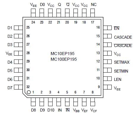
The MC100EP195 is a Programmable Delay Chip (PDC) designed primarily for clock deskewing and timing adjustment. It provides variable delay of a differential NECL/PECL input transition. The delay section consists of a programmable matrix of gates and multiplexers as shown in the logic diagram, Figure 2. The delay increment of the MC100EP195 has a digitally selectable resolution of about 10 ps and a net range of up to 10.2 ns. The required delay is selected by the 10 data select inputs D[9:0] values and controlled by the LEN (pin 10). A LOW level on LEN allows a transparent LOAD mode of real time delay values by D[9:0]. A LOW to HIGH transition on LEN will LOCK and HOLD current values present against any subsequent changes in D[10:0]. The approximate delay values for varying tap numbers correlating to D0 (LSB) through D9 (MSB) are shown in Table 6 and Figure 3.
Because the MC100EP195 is designed using a chain of multiplexers it has a fixed minimum delay of 2.2 ns. An additional pin D10 is provided for controlling Pins 14 and 15, CASCADE and CASCADE, also latched by LEN, in cascading multiple PDCs for increased programmable range. The cascade logic allows full control of multiple PDCs. Switching devices from all "1" states on D[0:9] with SETMAX LOW to all "0" states on D[0:9] with SETMAX HIGH will increase the delay equivalent to "D0", the minimum increment.
Select input pins D[10:0] may be threshold controlled by combinations of interconnects between VEF (pin 7) and VCF (pin 8) for LVCMOS, ECL, or LVTTL level signals. For LVCMOS input levels, leave VCF and VEF open. For ECL operation, short VCF and VEF (pins 7 and 8). For LVTTL level operation, connect a 1.5 V supply reference to VCF and leave open VEF pin. The 1.5 V reference voltage to VCF pin can be accomplished by placing a 2.2 k resistor between VCF and VEE for a 3.3 V power supply.
The VBB pin, an internally generated voltage supply, is available to
this MC100EP195 only. For single-ended input conditions, the unused
differential input is connected to VBB as a switching reference voltage.
VBB may also rebias AC coupled inputs. When used, decouple VBB
and VCC via a 0.01 F capacitor and limit current sourcing or sinking
to 0.5 mA. When not used, VBB should be left open.
The 100 Series contains temperature compensation.