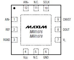
Features: · 1.8Msps· 50mW (ApplicationPinoutSpecificationsVDD to GND...........................................................-0.3V to +6VVL to GND .............-0.3V to the lower of (VDD + 0.3V) and +6VDigital Inputsto GND .................-0.3V to the lower of (VDD + 0.3V) and +6VDigital Output...
MAX1078: Features: · 1.8Msps· 50mW (ApplicationPinoutSpecificationsVDD to GND...........................................................-0.3V to +6VVL to GND .............-0.3V to the lower of (VDD + 0.3V) a...
SeekIC Buyer Protection PLUS - newly updated for 2013!
268 Transactions
All payment methods are secure and covered by SeekIC Buyer Protection PLUS.
VDD to GND...........................................................-0.3V to +6V
VL to GND .............-0.3V to the lower of (VDD + 0.3V) and +6V
Digital Inputs
to GND .................-0.3V to the lower of (VDD + 0.3V) and +6V
Digital Output
to GND....................-0.3V to the lower of (VL + 0.3V) and +6V
Analog Inputs and
REF to GND..........-0.3V to the lower of (VDD + 0.3V) and +6V
RGND to GND ....................................................-0.3V to +0.3V
Maximum Current into Any Pin.........................................50mA
Continuous Power Dissipation (TA = +70°C)
12-Pin TQFN (derate 16.9mW/°C above +70°C) ......1349mW
Operating Temperature Ranges
MAX107_ CTC ...................................................0°C to +70°C
MAX107_ ETC.................................................-40°C to +85°C
Junction Temperature..................................................+150°C
Storage Temperature Range .......................-60°C to +150°C
Lead Temperature (soldering, 10s) .............................+300°C
Stresses beyond those listed under "Absolute Maximum Ratings" may cause permanent damage to the device. These are stress ratings only, and functional operation of the device at these or any other conditions beyond those indicated in the operational sections of the specifications is not implied. Exposure to absolute maximum rating conditions for extended periods may affect device reliability.
The MAX1076/MAX1078 are low-power, high-speed, serial-output, 10-bit, analog-to-digital converters (ADCs) that operate at up to 1.8Msps and have an internal reference. These devices feature true-differential inputs, offering better noise immunity, distortion improvements, and a wider dynamic range over single-ended inputs. A standard SPI™/QSPI™/MICROWIRE™ interface provides the clock necessary for conversion. These devices easily interface with standard digital signal processor (DSP) synchronous serial interfaces.
The MAX1076/MAX1078 operate from a single +4.75V to +5.25V supply voltage. The MAX1076/MAX1078 include a 4.096V internal reference. The MAX1076 has a unipolar analog input, while the MAX1078 has a bipolar analog input. These devices feature a partial power-down mode and a full power-down mode for use between conversions, which lower the supply current to 2mA (typ) and 1µA (max), respectively. Also featured is a separate power-supply input (VL), which allows direct interfacing to +1.8V to VDD
digital logic.