Features: · Eight channel T1/E1/J1 long haul/short haul line interfaces
· Supports HPS (Hitless Protection Switching) for 1+1 protection without external relays
· Receiver sensitivity exceeds -36 dB@772KHz and -43 dB@1024 KHz
· Programmable T1/E1/J1 switchability allowing one bill of ma- terial for any line condition
· Single 3.3 V power supply with 5 V tolerance on digital interfaces
· Meets or exceeds specifications in
- ANSI T1.102, T1.403 and T1.408
- ITU I.431, G.703,G.736, G.775 and G.823
- ETSI 300-166, 300-233 and TBR 12/13
- AT&T Pub 62411
· Per channel software selectable on:
- Wave-shaping templates for short haul and long haul LBO (Line Build Out)
- Line terminating impedance (T1:100 Ω, J1:110 Ω, E1:75 Ω/120 Ω)
- Adjustment of arbitrary pulse shape
- JA (Jitter Attenuator) position (receive path or transmit path)
- Single rail/dual rail system interfaces
- B8ZS/HDB3/AMI line encoding/decoding
- Active edge of transmit clock (TCLK) and receive clock (RCLK)
- Active level of transmit data (TDATA) and receive data (RDATA)
- Receiver or transmitter power down
- High impedance setting for line drivers
- PRBS (Pseudo Random Bit Sequence) generation and detection with 215-1 PRBS polynomials for E1
- QRSS (Quasi Random Sequence Signals) generation and detection with 220-1 QRSS polynomials for T1/J1
- 16-bit BPV (Bipolar Pulse Violation)/Excess Zero/PRBS or QRSS error counter
- Analog loopback, Digital loopback, Remote loopback and Inband loopback
· Per channel cable attenuation indication
· Adaptive receive sensitivity
· Non-intrusive monitoring per ITU G.772 specification
· Short circuit protection for line drivers
· LOS (Loss Of Signal) & AIS (Alarm Indication Signal) detection
· JTAG interface
· Supports serial control interface, Motorola and Intel Non-Multi- plexed interfaces
· Package:
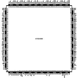
IDT82V2088: 208-pin PQFP and 208-pin PBGAPinout
Specifications
| Symbol |
Parameter |
Min |
Max |
Unit |
| VDDA, VDDD |
Core Power Supply |
-0.5 |
4.6 |
V |
| VDDIO |
I/O Power Supply |
-0.5 |
4.6 |
V |
| VDDT1-8 |
Transmit Power Supply |
-0.5 |
4.6 |
V |
| VDDR1-8 |
Receive Power Supply |
-0.5 |
4.6 |
|
| Vin |
Input Voltage, Any Digital Pin |
GND-0.5 |
5.5 |
V |
| Input Voltage, Any RTIP and RRING pin1 |
GND-0.5 |
VDDR+0.5 |
V |
| ESD Voltage, any pin 2000 2 V |
2000 2 |
|
V |
| |
|
V |
| Iin |
Transient latch-up current, any pin |
500 3 |
100 |
mA |
| Input current, any digital pin 4 |
|
10 |
mA |
| DC Input current, any analog pin 4 |
-10 |
±100 |
mA |
| Pd |
Maximum power dissipation in package DR208 |
|
3.35 |
W |
| Maximum power dissipation in package BB208 |
|
2.63 |
W |
| Tc |
Case Temperature |
|
120 |
°C |
| Ts |
Storage Temperature |
-65 |
+150 |
°C |
CAUTION:
Exceeding these values may cause permanent damage. Functional operation under these conditions is not implied. Exposure to absolute maximum rating conditions
for extended periods may affect device reliability. |
1.Reference to ground
2.Human body model
3.Charge device model
4.Constant input currentDescriptionThe IDT82V2088 can be configured as an octal T1, octal E1 or octal J1 Line Interface Unit. In receive path, an Adaptive Equalizer is integrated to remove the distortion introduced by the cable attenuation. The IDT82V2088 also performs clock/data recovery, AMI/B8ZS/HDB3 line decoding and detects and reports the LOS conditions. In transmit path, there is an AMI/ B8ZS/HDB3 encoder, Waveform Shaper and LBOs. There is one Jitter Attenuator for each channel, which can be placed in either the receive path or the transmit path. The Jitter Attenuator can also be disabled. The IDT82V2088 supports both Single Rail and Dual Rail system interfaces and both serial and parallel control interfaces. To facilitate the network mainte- nance, a PRBS/QRSS generation/detection circuit is integrated in each channel, and different types of loopbacks can be set on a per channel basis. Four different kinds of line terminating impedance, 75Ω, 100 Ω, 110 Ω and 120 Ω are selectable on a per channel basis. The chip also provides driver short-circuit protection and supports JTAG boundary scanning.
The IDT82V2088 can be used in SDH/SONET, LAN, WAN, Routers, Wireless Base Stations, IADs, IMAs, IMAPs, Gateways, Frame Relay Access Devices, CSU/DSU equipment, etc.

 IDT82V2088 Data Sheet


