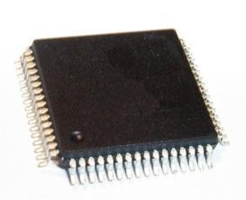
Features: •Fast access times: 10, 12 ns•Fast OE</a>access times: 5, 6, and 7 ns•Single +3.3V ±0.3V power supply•Fully static-no clock or timing strobes necessary•All inputs and outputs are TTL-compatible•Three state outputs•Center power and ground pi...
CY7C1041AV33: Features: •Fast access times: 10, 12 ns•Fast OE</a>access times: 5, 6, and 7 ns•Single +3.3V ±0.3V power supply•Fully static-no clock or timing strobes necessary•...
SeekIC Buyer Protection PLUS - newly updated for 2013!
268 Transactions
All payment methods are secure and covered by SeekIC Buyer Protection PLUS.
The CY7C1049AV33\GVT73512A8 is organized as a 262,144x 16 SRAM using a four-transistor memory cell with a high-per-formance, silicon gate, low-power CMOS process. Cypress SRAMs are fabricated using double-layer polysilicon, dou-ble-layer metal technology.
CY7C1041AV33 offers center power and ground pins for improved performance and noise immunity. Static design eliminates the need for external clocks or timing strobes. For increased sys-tem flexibility and eliminating bus contention problems, CY7C1041AV33 offers Chip Enable (CE</a>), separate Byte Enable controls (BLE</a> and BHE) and Output Enable (OE</a>) with this organization.
CY7C1041AV33 offers a low-power standby mode when chip is not selected. This allows system designers to meet low standby power requirements.