CD74HC4511

Features: 2-V to 6-V VCC Operation ('HC4511)4.5-V to 5.5-V VCC Operation (CD74HCT4511) High-Output Sourcing Capability− 7.5 mA at 4.5 V (CD74HCT4511)− 10 mA at 6 V ('HC4511) Input Latches for BCD Code Storage Lamp Test and Blanking Capability Balanced Propagation Delays and Transition...

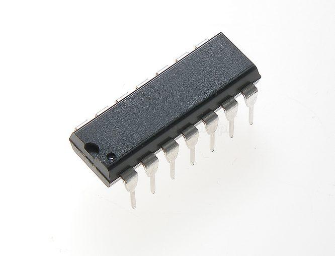
product image

CD74HC4511 Picture
SeekIC No. : 004312054 Detail

CD74HC4511: Features: 2-V to 6-V VCC Operation ('HC4511)4.5-V to 5.5-V VCC Operation (CD74HCT4511) High-Output Sourcing Capability− 7.5 mA at 4.5 V (CD74HCT4511)− 10 mA at 6 V ('HC4511) Input Latch...

floor Price/Ceiling Price

Part Number:
CD74HC4511
Supply Ability:
5000

Price Break

  • Qty
  • 1~5000
  • Unit Price
  • Negotiable
  • Processing time
  • 15 Days
Total Cost: $ 0.00

SeekIC Buyer Protection PLUS - newly updated for 2013!

  • Escrow Protection.
  • Guaranteed refunds.
  • Secure payments.
  • Learn more >>

Month Sales

268 Transactions

Rating

evaluate  (4.8 stars)

Upload time: 2024/11/21

Payment Methods

All payment methods are secure and covered by SeekIC Buyer Protection PLUS.

Notice: When you place an order, your payment is made to SeekIC and not to your seller. SeekIC only pays the seller after confirming you have received your order. We will also never share your payment details with your seller.
Product Details

Description


Features:

2-V to 6-V VCC Operation ('HC4511)
4.5-V to 5.5-V VCC Operation (CD74HCT4511)
High-Output Sourcing Capability
− 7.5 mA at 4.5 V (CD74HCT4511)
− 10 mA at 6 V ('HC4511)
Input Latches for BCD Code Storage
Lamp Test and Blanking Capability
Balanced Propagation Delays and Transition Times
Significant Power Reduction Compared to LSTTL Logic ICs
'HC4511
− High Noise Immunity,
NIL or NIH = 30% of VCC at VCC = 5 V
 CD74HCT4511
− Direct LSTTL Input Logic Compatibility,
VIL = 0.8 V Maximum, VIH = 2 V Minimum
− CMOS Input Compatibility, II 1 A at VOL, VOH


Pinout

  Connection Diagram


Specifications

Supply voltage range, VCC . . . . . . . . . . . . . . . . . . . . . . . . . . . . . . . . . . . . . . . . . . . . . . . . . . . . . . . . . . −0.5 V to 7 V
Input diode current, IIK (VI < −0.5 V or VI > VCC + 0.5 V) ) (see Note 1) . . . . . . . . . . . . . . . . . . . . . . . . ±20 mA
Output diode current, IOK (VO < −0.5 V or VO > VCC + 0.5V) (see Note 1) . . . . . . . . . . . . . . . . . . . . . . ±20 mA
Continuous output source or sink current per output, IO (VO = 0 to VCC) . . . . . . . . . . . . . . . . . . . . . . . ±25 mA
Continuous current through VCC or GND . . . . . . . . . . . . . . . . . . . . . . . . . . . . . . . . . . . . . . . . . . . . . . . . . . . ±50 mA
Package thermal impedance, JA (see Note 2): E package . . . . . . . . . . . . . . . . . . . . . . . . . . . . . . . . . . . 67/W
                                                                          M package . . . . . . . . . . . . . . . . . . . . . . . . . . . . . . . . . . 73/W
                                                                          PW package . . . . . . . . . . . . . . . . . . . . . . . . . . . . . . . . 108/W
Lead temperature (during soldering):
At distance 1/16 ± 1/32 in (1.59 ± 0.79 mm) from case for 10 s maximum . . . . . . . . . . . . . . . . . . . . . 265
Unit inserted into a PC board (minimum thickness 1/16 in, 1.59 mm),
with solder contacting lead tips only . . . . . . . . . . . . . . . . . . . . . . . . . . . . . . . . . . . . . . . . . . . . . . . . . . . 300Storage temperature, Tstg . . . . . . . . . . . . . . . . . . . . . . . . . . . . . . . . . . . . . . . . . . . . . . . . . . . . . . . . . . . −65 to 150
† Stresses beyond those listed under "absolute maximum ratings" may cause permanent damage to the device. These are stress ratings only, and functional operation of the device at these or any other conditions beyond those indicated under "recommended operating conditions" is not implied. Exposure to absolute-maximum-rated conditions for extended periods may affect device reliability.
NOTES: 1. The input and output voltage ratings may be exceeded if the input and output current ratings are observed.
2. The package thermal impedance is calculated in accordance with JESD 51-7.


Description

The CD54HC4511, CD74HC4511, and CD74HCT4511 are BCD-to-7 segment latch/decoder/drivers with four address inputs (D0−D3), an active-low blanking (BL) input, lamp-test (LT) input, and a latch-enable (LE) input that, when high, enables the latches to store the BCD inputs. When LE is low, the latches are disabled, making the outputs transparent to the BCD inputs.

CD74HC4511 have standard-size output transistors, but are capable of sourcing (at standard VOH levels) up to 7.5 mA at 4.5 V. The HC types can supply up to 10 mA at 6 V.


Customers Who Bought This Item Also Bought

Margin,quality,low-cost products with low minimum orders. Secure your online payments with SeekIC Buyer Protection.
Industrial Controls, Meters
Crystals and Oscillators
Static Control, ESD, Clean Room Products
Resistors
Integrated Circuits (ICs)
View more