703039Y

Features: . Number of instructions: 74. Minimum instruction execution time:*62.5 ns (@ 16 MHz operation with main system clock)*30.5 µs (@ 32.768 kHz operation with subsystem clock). General-purpose registers: 32 bits ×32 registers. Instruction set (signed multiplication, saturationoperation...

product image

703039Y Picture
SeekIC No. : 004239826 Detail

703039Y: Features: . Number of instructions: 74. Minimum instruction execution time:*62.5 ns (@ 16 MHz operation with main system clock)*30.5 µs (@ 32.768 kHz operation with subsystem clock). General-p...

floor Price/Ceiling Price

Part Number:
703039Y
Supply Ability:
5000

Price Break

  • Qty
  • 1~5000
  • Unit Price
  • Negotiable
  • Processing time
  • 15 Days
Total Cost: $ 0.00

SeekIC Buyer Protection PLUS - newly updated for 2013!

  • Escrow Protection.
  • Guaranteed refunds.
  • Secure payments.
  • Learn more >>

Month Sales

268 Transactions

Rating

evaluate  (4.8 stars)

Upload time: 2024/11/21

Payment Methods

All payment methods are secure and covered by SeekIC Buyer Protection PLUS.

Notice: When you place an order, your payment is made to SeekIC and not to your seller. SeekIC only pays the seller after confirming you have received your order. We will also never share your payment details with your seller.
Product Details

Description


Features:

. Number of instructions:  74
. Minimum instruction execution time:
*62.5 ns (@ 16 MHz operation with main system clock)
*30.5 µs (@ 32.768 kHz operation with subsystem clock)
. General-purpose registers:  32 bits × 32 registers
. Instruction set (signed multiplication, saturationoperations, 32-bit shift instructions, bit manipulationinstructions, load/store instructions)
. Memory space:16 MB linear address spaceMemory block allocation function:  2 MB per block
. External bus:  16-bit multiplexed bus
. Internal memory:
*µPD703039, 703039Y(ROM: 256 KB, RAM: 8 KB)
*µPD703040, 703040Y(ROM: 256 KB, RAM: 16 KB)
*µPD703041, 703041Y(ROM: 192 KB, RAM: 8 KB)
. I/O lines  Total:  151
. 10-bit resolution A/D converter:  16 channels
. Timer/counter
*24-bit: 2 channels, 16-bit: 2 channels
*8-bit: 8 channels
. Watch timer:  1 channel
. Watchdog timer:  1 channel
. DMA controller:  6 channels
. Interrupts and exceptionsNon-maskable interrupt: 2 sourcesMaskable interrupt
: µPD703039, 703040, 703041 (51 sources)
: µPD703039Y, 703040Y, 703041Y (52 sources)
*Software exception: 32 sourcesException trap: 1 source
. Serial interface (SIO)Asynchronous serial interface (UART)Clocked serial interface (CSI)3-wire variable length serial interface (CSI4)I2C bus
   interface (I2C) (µPD703039Y, 703040Y,703041Y)
. RTP:  8 bits × 2 channels or 4 bits × 4 channels


Application

*System/servo/camera control of camcorders
*Portable cameras such as digital still cameras
*Cellular phones, portable information terminals, etc.


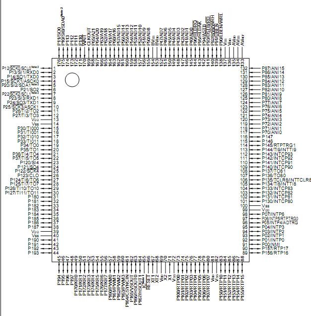
Pinout

  Connection Diagram


Specifications

Parameter Symbol Conditions Ratings Unit
Supply voltage VDD
  0.5 to +4.6 V
AVDD
  0.5 to +4.6 V
BVDD   0.5 to +4.6 V
AVSS   0.5 to +0.5 V
BVSS   0.5 to +0.5 V
Input voltage VI1 Note 1(VDD) 0.5 to VDD + 0.5Note 4 V
VI2 Note 2(BVDD) 0.5 to BVDD + 0.5Note 4 V
Clock input voltage VK X1, XT1, VDD= 2.7 to 3.6 V 0.5 to VDD + 1.0Note 4  
Analog input voltage VIAN Note 3(AVDD) 0.5 to AVDD + 0.5Note 4 V
Analog reference input voltage AVREF AVREFpin
0.5 to AVDD + 0.5Note 4 V
Output current, low IOL Per pin 4.0 mA
Total for P00 to P07, P150 toP157 25 mA
Total for P100 to P107, P160 to P167 25 mA
Total for P170 to P177, P190 to P197 25 mA
Total for P124 to P127, P180 to P187 25 mA
Total for P30 to P37, P120 to P123 25 mA
Total for P12 to P15, P20 to P27, P110 toP113 25 mA
Total for P50 to P57, P60 to P65, CLKOUT 25 mA
Total for P40 to P47, P90 to P96 25 mA
Total for P130 to P137, P140 to P147 25 mA
Output current, high IOH Per pin 4.0 mA
Total for P00 to P07, P150 to P157 25 mA
Total for P100 to P107, P160 to P167 25 mA
Total for P170 to P177, P190 to P197 25 mA
Total for P124 to P127, P180 to P187 25 mA
Total for P30 to P37, P120 to P123 25 mA
Total for P12 to P15, P20 to P27, P110 toP113 25 mA
Total for P50 to P57, P60 to P65, CLKOUT 25 mA
Total for P40 to P47, P90 to P96 25 mA
Total for P130 to P137, P140 to P147 25 mA
Output voltage VO1 Note 1(VDD) 0.5 to VDD + 0.5 V
VO2
Note 2 (BVDD) 0.5 to BVDD + 0.5 V
Operating ambient temperature TA   40 to +85 °C
Storage temperature Tstg   65 to +150 °C


Description

The µPD703039, 703039Y, 703040, 703040Y, 703041, and 703041Y (collectively known as the V850/SV1) areproducts in the low-power series of V850 FamilyTMproducts, which are NEC's single-chip microcontrollers for real-time control.

The V850/SV1 employs the CPU core of the V850 Family, and has on-chip peripheral functions such as largecapacity ROM/RAM, a multi-function timer/counter, serial interface, A/D converter, DMA controller, PWM, and aVsync/Hsync separation circuit.

The V850/SV1 not only realizes the low power consumption necessary for applications such as camcorders, butalso extremely high cost performance.

Detailed function descriptions of V850/SV1 are provided in the following user's manuals.  Be sure to read them beforedesigning.
V850/SV1 User's Manual  Hardware:  U14462E
V850 Family User's Manual  Architecture:  U10243E


Customers Who Bought This Item Also Bought

Margin,quality,low-cost products with low minimum orders. Secure your online payments with SeekIC Buyer Protection.
Transformers
Fans, Thermal Management
Integrated Circuits (ICs)
Circuit Protection
View more