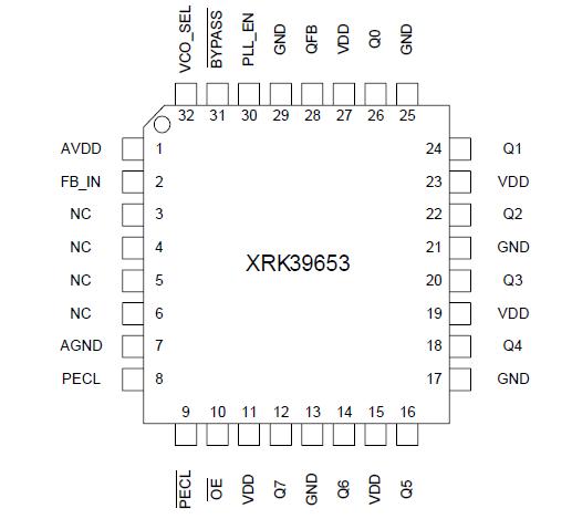
Features: • 8 LVCMOS Clock Outputs• 1 Feedback Output• LVPECL reference clock input• 25-125 MHz input/output frequency range Input/Output range (÷4): 50-125MHz Input/Output range (÷8): 25-62.5MHz• 150ps max output to output skew• Two bypass test mode options...
XRK39653: Features: • 8 LVCMOS Clock Outputs• 1 Feedback Output• LVPECL reference clock input• 25-125 MHz input/output frequency range Input/Output range (÷4): 50-125MHz Input/Output...
SeekIC Buyer Protection PLUS - newly updated for 2013!
268 Transactions
All payment methods are secure and covered by SeekIC Buyer Protection PLUS.
SYMBOL |
CHARACTERISTICS |
MIN |
MAX |
UNIT |
CONDITION |
VDD |
Supply Voltage |
-0.3 |
3.9 |
V |
|
VIN |
DC Input Voltage |
-0.3 |
VDD + 0.3 |
V |
|
VOUT |
DC Output Voltage |
-0.3 |
VDD + 0.3 |
V |
|
IIN |
DC Input Current |
±20 |
mA |
||
IOUT |
DC Output Current |
±50 |
mA |
||
TS |
Storage Temperature |
-65 |
125 |
°C |
a. Absolute maximum continuous ratings are those maximum values beyond which damage to the device may occur.
Exposure to these conditions or conditions beyond those indicated may adversely affect device reliability.
The XRK39653 is a low voltage high performance PLL based zero delay buffer/clock generator designed for high speed clock distribution applications. It provides 9 low skew, low jitter outputs ideal for networking, computing and telecom applications.
The PLL based design allows the 9 outputs (8 clock outputs and 1 feedback output) to be phase aligned to the input reference clock. The outputs source LVCMOS compatible levels and can drive 50 transmission lines. If series termination is used, each output can drive up to 2 lines providing effectively a fanout of 1:16. The XRK39653's reference input accepts a LVPECL clock source.
For normal operation (PLL used to source the outputs), the feedback output (QFB) is connected to the feedback input (FB_IN). The VCO range of operation is 200 to 500MHz. This means that the input/output ranges are determined by the divider setting. If ÷4 is used, the input/output range is 50 to 125MHz (high range), if ÷8 is used the input/output range is 25 to 62.5MHz (low range).
For testing purposes two PLL bypass modes are provided. The first simply replaces the PLL output with the reference clock (PLL_EN=0, BYPASS=1). The dividers are still in use. The second is a full bypass mode that has the PLL and divider operation removed (BYPASS=0). In this mode the reference clock directly sources the outputs drivers.