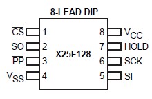
Features: • 1MHz Clock Rate
• SPI Serial Interface
• 16K X 8 Bits
-32 Byte Small Sector Program Mode
• Low Power CMOS
-<1mA Standby Current
-<5mA Active Current
• 1.8V 3.6V or 5V "Univolt" Read and Program Power Supply Versions
• Block Lock Protection
-Protect 1/4, 1/2 or all of E2PROM Array
• Built-in Inadvertent Program Protection
-Power-Up/Power-Down protection circuitry
-Program Enable Latch
-Program Protect Pin
• Self-Timed Program Cycle
-5ms Program Cycle Time (Maximum)
• High Reliability
-Endurance: 100,000 cycles per byte
-Data Retention: 100 Years
-ESD protection: 2000V on all pins
• 8-Lead PDlP Package
• 16-Lead 150 mil SOIC Package
Pinout Specifications
Temperature Under Bias .................. 65 to +135
Storage Temperature ....................... 65 to +150
Voltage on any Pin with Respect to VSS ... 1V to +7V
D.C. Output Current ............................................5mA
Lead Temperature
(Soldering, 10 Seconds) ................................... 300
Stresses above those listed under "Absolute Maximum Ratings" may cause permanent damage to the device.
This is a stress rating only and the functional operation of the device at these or any other conditions above those listed in the operational sections of this specification is not implied. Exposure to absolute maximum rating conditions for extended periods may affect device reliability.
DescriptionThe X25F128 is a 131,072-bit CMOS SerialFlash memory, internally organized 16K X 8. It features a "Univolt" Program and Read voltage, Serial Peripheral Interface (SPI), and software protocol allowing operation on a simple three-wire bus. The bus signals are a clock input (SCK), plus separate data in (SI) and data out (SO) lines. Access to the device is controlled through a chip select (CS) input, allowing any number of devices to share the same bus.
The X25F128 also features two additional inputs that provide the end user with added flexibility. By asserting the HOLD input, the X25F128 will ignore transitions on its inputs, thus allowing the host to service higher priority interrupts. The PP input can be used as a hardwire input to the X25F128 disabling all program attempts to the status register, thus providing a mechanism for limiting end user capability of altering 0, 1/4, 1/2, or all of the memory.
The X25F128 utilizes Xicor's proprietary flash cell, providing a minimum endurance of 100,000 cycles and a minimum data retention of 100 years.

 X25F128 Data Sheet


