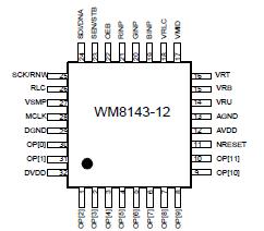
Features: · Reset level clamp
· Correlated double sampling (CDS)
· Fine offset level shifting
· Programmable gain amplification
· 12-bit ADC with maximum 4 MSPS
· Simple clocking scheme
· Control by serial or parallel interface
· Time multiplexed eight-bit data output mode
· 32 pin TQFP package
· Interface compatible with WM8144-10 andWM8144-12Application· Flatbed scanners
· Sheet feed scanners
· Film scanners
· CCD sensor interfaces
· Contact image sensor (CIS) interfacesPinout Specifications
Analogue Supply Voltage ...... AGND - 0.3V, AGND +7V
Digital Supply Voltage ............DGND - 0.3V, DGND +7V
Digital Inputs ...................... DGND - 0.3V, DVDD +0.3V
Digital Outputs .................... DGND - 0.3V, DVDD +0.3V
Reference Inputs ..................AGND - 0.3V, AVDD +0.3V
RINP, GINP, BINP..................AGND - 0.3 V, AVDD +0.3V
Operating Temperature Range, TA ....... 0°C to +70°C
Storage Temperature....................... -50°C to +150°C
Lead Temperature (10 second soldering)....... +260°C
DescriptionThe WM8143-12 integrates the analogue signalconditioning required by CCD sensors with a 12-bit ADC.The WM8143-12 requires minimal external circuitry andprovides a cost-effective sensor to digital domain systemsolution.
Each of the three analogue conditioning channelsincludes reset level clamp, CDS, fine offset level shiftingand programmable gain amplification. The three channelsare multiplexed into the ADC. The output from the ADC isfed to the output bus pins OP[11:0] via a 12/8 bitmultiplexer, enabled by the OEB signal.
The flexible output architecture of the WM8143-12 allows twelve-bit data tobe accessed either on a twelve-bit bus or via a timemultiplexedeight-bit bus. The WM8143-12 can beconfigured for pixel-by-pixel or line-by-line multiplexingoperation. Reset level clamp and/or CDS features can beoptionally bypassed. The device configuration isprogrammed either via a simple serial interface or via aneight-bit parallel interface.
The serial/parallel interfaces of the WM8143-12 arecontrol compatible with those of the WM8144-10 andWM8144-12.

 WM8143-12 Data Sheet


