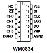
Features: • Functionally Equivalent to National Semiconductor ADC0834 and ADC0838 without the Internal Zener Regulator Network
• 4-input (WM0834) or 8-input (WM0838) MUX options
• Reference input operates ratiometrically or with a fixed reference
• Input range 0 to Vcc with Vcc Reference
• 5V and 3.3V variants
• Total Unadjusted Error: ± 1 LSB
• 8-bit resolution
• Low Power
• 32 ms conversion time at fclock = 250 kHz
• Serial I/O interface
• WM0834 packages: 14 pin SO & DIP WM0838 packages: 20 pin wide-body SO & DIP
Application• Embedding with remote sensors
• Equipment health monitoring
• Automotive
• Industrial control
Pinout Specifications
Supply Voltage, Vcc (note 2) . . . . . . . . . . . . . . 6.5 V
Input voltage range:
Digital Inputs . . . . . . . . . . GND - 0.3 V, VCC + 0.3 V
Analogue inputs . . . . . . .. GND - 0.3 V, VCC + 0.3 V
Input current, any pin (note 3) . . . . . . . . . .± 5 mA
Total Input current for package . . . . . . . .. ± 20 mA
Operating temperature range, TA . . . TMIN to TMAX
WM083_C_ (C suffix) . . . . . . . . . . . . . 0oC to +70oC
WM083_I_ (I suffix) . . . . . . . . . . . . -40oC to +85oC
Storage Temperature . . . . . . . . . - 65oC to +150oC
Soldering Information:
Lead Temperature 1.6 mm (1/16) from case
for 10 seconds: D, DW or N package . . . . . . . 260oC
DescriptionWM0834 and WM0838 are 8-bit analogue to digital converters (ADC) with configurable 4-input and 8-input multiplexers respectively and a serial I/O interface.
Assignment of the multiplexer inputs is configured before each conversion via the serial data input to give single-ended or differential operation for the selected inputs. A mixture of input configurations can be used in the same application. WM0838 also has a pseudo-differential configuration where all 8 inputs can be refered to a common input at an arbitrary voltage.
Serial communcation with WM0834/8 is via Data In (DI) and Data Out (DO) wires under the control of clock and chip select inputs. A high output at the SARS pin indicates when the conversion is in progress. To initiate a conversion chip enable is held low and data is input to DI on the rising edge of the clock, comprising, a start bit, and bits to set up the input configuration and polarity. After a half clock cycle delay conversion results appear at DO on the falling edge of the clock, MSB first, concurrently with A-D conversion. This is followed by the results LSB first, indicated by the falling edge of SARS. WM0838 has a shift enable (SE) input used to control the LSB first output on DO.
WM0834/8 operate on 5V and 3.3V supply voltages and are available in small outline and DIP packages for commercial (0 to 70OC) and industrial (-40 to 85OC) temperature ranges.

 WM0834 Data Sheet


