WEDF1M32B-XXX5

Features: ` Access Times of 70, 90, 120ns` Packaging: • 66 pin, PGA Type, 1.185 square, Hermetic Ceramic HIP (Package 401) • 68 lead, 22mm Low Profi le CQFP, 4.6mm (0.180 ), (Package 509)` Sector Architecture • One 16KByte Sectors • Two 8KByte Sectors • One 32KByte S...

product image

WEDF1M32B-XXX5 Picture
SeekIC No. : 004545608 Detail

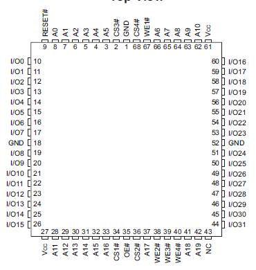
WEDF1M32B-XXX5: Features: ` Access Times of 70, 90, 120ns` Packaging: • 66 pin, PGA Type, 1.185 square, Hermetic Ceramic HIP (Package 401) • 68 lead, 22mm Low Profi le CQFP, 4.6mm (0.180 ), (Package 50...

floor Price/Ceiling Price

Part Number:
WEDF1M32B-XXX5
Supply Ability:
5000

Price Break

  • Qty
  • 1~5000
  • Unit Price
  • Negotiable
  • Processing time
  • 15 Days
Total Cost: $ 0.00

SeekIC Buyer Protection PLUS - newly updated for 2013!

  • Escrow Protection.
  • Guaranteed refunds.
  • Secure payments.
  • Learn more >>

Month Sales

268 Transactions

Rating

evaluate  (4.8 stars)

Upload time: 2024/5/16

Payment Methods

All payment methods are secure and covered by SeekIC Buyer Protection PLUS.

Notice: When you place an order, your payment is made to SeekIC and not to your seller. SeekIC only pays the seller after confirming you have received your order. We will also never share your payment details with your seller.
Product Details

Description


Features:

` Access Times of 70, 90, 120ns
` Packaging:
   • 66 pin, PGA Type, 1.185" square, Hermetic Ceramic HIP (Package 401)
   • 68 lead, 22mm Low Profi le CQFP, 4.6mm (0.180"), (Package 509)
` Sector Architecture
   • One 16KByte Sectors
   • Two 8KByte Sectors
   • One 32KByte Sectors
   • Fifteen 64KByte Sectors
` 1,000,000 Erase/Program Cycles
` Organized as 1Mx32, user confi gurable as 2Mx16 or 4Mx8.
` Commercial, Industrial and Military Temperature Ranges
` 5V ± 10% for Read and Write Operations.
` Low Power CMOS
` Embedded Erase and Program Algorithm
` Built-in Decoupling Caps and Multiple Ground Pins for Low Noise Operation
` Weight
     WEDF1M32B-XG2TX5 - 8 grams typical
     WEDF1M32B-XHX5 - 13 grams typical
* This product is under development, is not qualifi ed or characterized and is subject to change or cancellation without notice.


Pinout

  Connection Diagram


Specifications

Parameter
Unit
Voltage on Any Pin with Respect to
GNDVCC and VPP
-0.5 to +7.0
V
Voltage with Respect to GND A9, OE#, and
RESET (2)
-2.0 to +12.5
V
Voltage with Respect to GND All other
pins (1)
-2.0 to +7.0
V
Output Short Circuit Current
200
mA

NOTES:
1. Minimum DC voltage is -0.5V on input/output pins. During transitions, this level may undershoot to -2.0V for periods <20ns. Maximum DC voltage on input/output pins is VCC + 0.5V which, during transitions, may overshoot to VCC + 2.0V for periods <20ns.
2. Minimum DC input voltage on pins A9, OE#, and RESET is -0.5V. During voltage transitions, A9, OE#, and RESET may undershoot Vss to -2.0V for periods of up to 20ns. See Figure 6. Maximum DC input voltage on pin A9 is +12.5V which may overshoot to +13.5V for periods up to 20ns.
3. Output shorted for no more than one second. No more than one output shorted at a time.

Stresses above those listed under "Absolute Maximum Ratings" may cause permanent damage to the device. This is a Stress rating only and functional operation of the device at these or any other conditions above those indicated in the operational sections of this specifi cation is not implied. Exposure to absolute maximum rating conditions for extended periods may affect device reliability.


Customers Who Bought This Item Also Bought

Margin,quality,low-cost products with low minimum orders. Secure your online payments with SeekIC Buyer Protection.
Sensors, Transducers
Discrete Semiconductor Products
Static Control, ESD, Clean Room Products
Optoelectronics
Boxes, Enclosures, Racks
Potentiometers, Variable Resistors
View more