VSC8479

Features: `16:1 Mux/Demux Transceiver With Integrated Clock Multiplier Unit, and Clock and Data Recov-ery Unit with Limiting Amplifier`0.13m CMOS Process Technology`XFI Output Compliance Mode for XFP Modules`Programmable Input Signal Bandwidth Equalization (EQ)- Enhanced Optical Performance- Enhan...

product image

VSC8479 Picture
SeekIC No. : 004543481 Detail

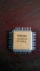
VSC8479: Features: `16:1 Mux/Demux Transceiver With Integrated Clock Multiplier Unit, and Clock and Data Recov-ery Unit with Limiting Amplifier`0.13m CMOS Process Technology`XFI Output Compliance Mode for XF...

floor Price/Ceiling Price

Part Number:
VSC8479
Supply Ability:
5000

Price Break

  • Qty
  • 1~5000
  • Unit Price
  • Negotiable
  • Processing time
  • 15 Days
Total Cost: $ 0.00

SeekIC Buyer Protection PLUS - newly updated for 2013!

  • Escrow Protection.
  • Guaranteed refunds.
  • Secure payments.
  • Learn more >>

Month Sales

268 Transactions

Rating

evaluate  (4.8 stars)

Upload time: 2024/5/10

Payment Methods

All payment methods are secure and covered by SeekIC Buyer Protection PLUS.

Notice: When you place an order, your payment is made to SeekIC and not to your seller. SeekIC only pays the seller after confirming you have received your order. We will also never share your payment details with your seller.
Product Details

Description


Features:

`16:1 Mux/Demux Transceiver With Integrated Clock Multiplier Unit, and Clock and Data Recov-ery Unit with Limiting Amplifier
`0.13m CMOS Process Technology
`XFI Output Compliance Mode for XFP Modules
`Programmable Input Signal Bandwidth Equalization (EQ)
- Enhanced Optical Performance
- Enhanced XFI Stressed Eye Performance
`Built-in Self-test Generation and Error Detection:
- Industry Standard PRBS Generation and Detection
- User Defined Patterns
`Full Support for 300-Pin MSA Transponder Modules:
- Multiple Reference Clock Source Inputs and Selectable Frequencies
- Facility and Equipment Loopback Modes
- Support for Line Timing Mode with Clock Clean-up
- Loss of Lock (LOL) and FIFO Alarm Outputs
- Adjustable Loss of Signal (LOS) Alarm
`Two-wire or SPI Micro-controller Serial Interface Port (selectable)
- Programmable Registers for Access to All Control/Status Signals
`TxRef Clock, RxRef Clock and ExRef Clock Sources
- Flexible Reference Clock Routing
- Reference Clock "Clean-up" Phase Detector
`Selectable Duobinary Modulation Pre-Coder
`Programmable High-speed Input Voltage Offset Adjust
`High-speed Data Inversion and Low-Speed Bit Order Swap
`High-speed CML Clock Output with Power Down Mode


Application

·􀀗XFP Module XFI to Host SERDES Applications
·􀀗300 Pin MSA Transponder Modules
·􀀗10GE and Fibre Channel to SFI-4 SERDES Applications
·􀀗SONET/SDH and DWDM Systems


Description

The VSC8479 is a 1:16, 16:1 transceiver with integrated Clock and Data Recovery unit (CDR) and Clock Multiplier Unit (CMU) that provides the most comprehensive solution available in the industry. Continuous frequency of operation spans from 9.953 Gbps to 11.3 Gbps over full temperature range.

Targeted for XFP Host ASIC SERDES, 300 pin module and DWDM line card applications, the VSC8479 provides industry leading optimization of power, performance, programmability, price and feature integration. The 1.15 W total power dissipation enables 300 pin MSA module vendors to provide performance and functionality advantages while dropping the overall power dissipation of their existing modules. The VSC8479 is a perfect choice for XFP motherboards with proven inter-operability with all major XFP module vendors.

The receiver path has a high sensitivity receiver with a programmable VGA and input bandwidth equalization (EQ) to provide stressed input data eye compensation. No external post amplifier is required for most applications.

The high-speed output is swing and pre-emphasis programmable to support a variety laser driver and XFI host ASIC applications.

The VSC8479 fully supports all features, functions and clock modes required for 300-pin multi-source agreement (MSA) transponder module full compliance. All loopback modes are supported with multiple line timing clock modes.

A highly flexible reference clock source selection and reference clock clean-up support scheme is provided to minimize external circuitry. A selectable two-wire serial or Serial Peripheral Interface (SPI) provides full microcontroller access to all status and control registers, including software read-back capability of all external control input pins. Any combination of discrete pins and serial register status and control can be employed. A highly flexible PRBS and user defined pattern checker and error count provides system analysis and built-in self-testing.

Robust cross talk immunity enables the VSC8479 to operate the Tx and Rx paths asynchronously to each other while exceeding SONET level jitter generation and jitter tolerance performance. A high-speed output clock can be optionally enabled for higher performance applications. An adjustable loss of signal (LOS) indicator is integrated into the device enabling optical modulation amplitude monitoring.

The power supply scheme provides a high degree of flexibility. The device can operate on a single +1.8V supply with an optional +3.3V I/O supply for 3.3V compliant interfacing. The Tx path and Rx path can be powered down independently. The single chip, small footprint (17 x 17 mm) allows for both cost reduction and board size reduction for price and size aggressive, small form factor module applications. All VSC8479 devices are tested at high-speed to insure the highest performance and quality standards you've come to expect from Vitesse.


Customers Who Bought This Item Also Bought

Margin,quality,low-cost products with low minimum orders. Secure your online payments with SeekIC Buyer Protection.
Connectors, Interconnects
Batteries, Chargers, Holders
Motors, Solenoids, Driver Boards/Modules
Transformers
Tapes, Adhesives
803
View more