VSC8124

Features: • Four Channel 2.488 Gb/s Data Recovery• SONET Quality Jitter Tolerance• Fastlock Data Acquisition less than 200 Bit Times• Loss of Signal Indicators• Long Strings of Static Data Tolerated by the Clock Recovery Circuit without Loss of Signal• First Ord...

product image

VSC8124 Picture
SeekIC No. : 004543445 Detail

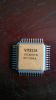
VSC8124: Features: • Four Channel 2.488 Gb/s Data Recovery• SONET Quality Jitter Tolerance• Fastlock Data Acquisition less than 200 Bit Times• Loss of Signal Indicators• Long St...

floor Price/Ceiling Price
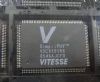
Part Number:
VSC8124
Supply Ability:
5000

Price Break

  • Qty
  • 1~5000
  • Unit Price
  • Negotiable
  • Processing time
  • 15 Days
Total Cost: $ 0.00

SeekIC Buyer Protection PLUS - newly updated for 2013!

  • Escrow Protection.
  • Guaranteed refunds.
  • Secure payments.
  • Learn more >>

Month Sales

268 Transactions

Rating

evaluate  (4.8 stars)

Upload time: 2024/5/10

Payment Methods

All payment methods are secure and covered by SeekIC Buyer Protection PLUS.

Notice: When you place an order, your payment is made to SeekIC and not to your seller. SeekIC only pays the seller after confirming you have received your order. We will also never share your payment details with your seller.
Product Details

Description


Features:

• Four Channel 2.488 Gb/s Data Recovery
• SONET Quality Jitter Tolerance
• Fastlock Data Acquisition less than 200 Bit Times
• Loss of Signal Indicators
• Long Strings of Static Data Tolerated by the Clock Recovery Circuit without Loss of Signal
• First Order Clock Recovery Loop Minimizes Jitter Accumulation
• Differential on Chip Terminated Serial Data I/O
• Bypass for OC3, OC12 Data Rates
• 155.52 MHz Reference Clock Frequency
• 3.3V Supply Operation
• 14 x 14mm, 100 Pin Thermally Enhanced TQFP Package


Pinout

  Connection Diagram


Specifications

Power Supply Voltage, (VCC) ...........................-0.5 V to +4.0 V
DC Input Voltage (Differential inputs) .......-0.5 V to VCC + 0.5V
DC Input Voltage (TTL inputs).................. -0.5 V to VCC + 0.5 V
DC Output Voltage (TTL outputs ...............-0.5 V to VCC + 0.5V
Output Current (TTL outputs) .....................................+/- 50mA
Output Current (Differential outputs)..........................+/- 50mA
Case Temperature Under Bias..........................-55 to + 100

Note: Caution: Stresses listed under "Absolute Maximum Ratings" may be applied to devices one at a time without causing permanent damage. Functionality at or exceeding the values listed is not implied. Exposure to these values for extended periods may affect device reliability.


Description

The VSC8124 is a four channel, 2.5 Gb/s data re-timer for cleaning up data downstream of optical links or cross point switches. Serial data at the 2.5 Gb/s rate is independently re-timed on four channels, and driven differentially by CML drivers. The re-timing function on each channel can be individually bypassed for lower rate signals or test purposes. The VSC8124 provides four independent loss of signal indicators in the event of loss of synchronous data transitions.


Customers Who Bought This Item Also Bought

Margin,quality,low-cost products with low minimum orders. Secure your online payments with SeekIC Buyer Protection.
Memory Cards, Modules
Soldering, Desoldering, Rework Products
Power Supplies - Board Mount
Prototyping Products
DE1
View more