VSC8115

Features: • Performs clock and data recovery for 622.08Mb/s (STS-12/OC-12/STM-4) or 155.52Mb/s (STS-3/OC-3/STM-1) NRZ data• Meets Bellcore, ITU and ANSI Specifications for Jitter Performance• 19.44MHz reference frequency LVTTL Input• Lock Detect output pin monitors data run...

product image

VSC8115 Picture
SeekIC No. : 004543439 Detail

VSC8115: Features: • Performs clock and data recovery for 622.08Mb/s (STS-12/OC-12/STM-4) or 155.52Mb/s (STS-3/OC-3/STM-1) NRZ data• Meets Bellcore, ITU and ANSI Specifications for Jitter Perform...

floor Price/Ceiling Price

Part Number:
VSC8115
Supply Ability:
5000

Price Break

  • Qty
  • 1~5000
  • Unit Price
  • Negotiable
  • Processing time
  • 15 Days
Total Cost: $ 0.00

SeekIC Buyer Protection PLUS - newly updated for 2013!

  • Escrow Protection.
  • Guaranteed refunds.
  • Secure payments.
  • Learn more >>

Month Sales

268 Transactions

Rating

evaluate  (4.8 stars)

Upload time: 2024/11/23

Payment Methods

All payment methods are secure and covered by SeekIC Buyer Protection PLUS.

Notice: When you place an order, your payment is made to SeekIC and not to your seller. SeekIC only pays the seller after confirming you have received your order. We will also never share your payment details with your seller.
Product Details

Description


Features:

• Performs clock and data recovery for 622.08Mb/s (STS-12/OC-12/STM-4) or 155.52Mb/s (STS-3/OC-3/STM-1) NRZ data
• Meets Bellcore, ITU and ANSI Specifications for Jitter Performance
• 19.44MHz reference frequency LVTTL Input
• Lock Detect output pin monitors data run length and frequency drift from the reference clock
• Data is Retimed at the Output
• Active High Signal Detect LVPECL Input
• Low-jitter high speed outputs can be configured as either LVPECL or low power LVDS
• Low power - 0.188 Watts Typical Power
• +3.3V Power Supply
• 20 Pin TSSOP Package
• Requires One External Capacitor
• PLL bypass operation facilitates the board debug process


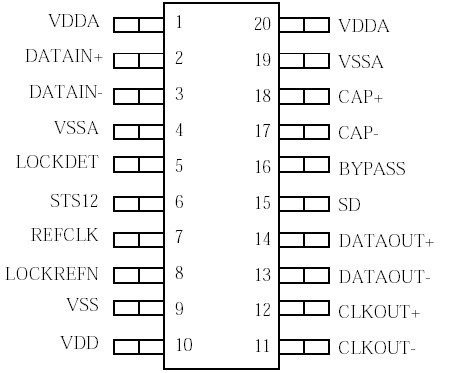
Pinout

  Connection Diagram


Specifications

Power Supply Voltage (VDD) Potential to GND......................................................................-0.5V to +4V
DC Input Voltage (LVPECL Inputs)........................................................................... -0.5V to VDD + 0.5V
DC Input Voltage (LVTTL Inputs) ............................................................................. -0.5V to VDD + 0.5V
Output Current (LVDS or LVPECL Outputs)................................................................................ +/-50mA
Case Temperature Under Bias.........................................................................................-55o to +125
Storage Temperature .................................................................................................. -65oC to +150
Maximum Input ESD (Human Body Model)
High Speed Outputs (pins 11, 12, 13, & 14) ................................................................................... 500V
All Other Pins ................................................................................................................................ 1500V


Description

The VSC8115 functions as a clock and data recovery unit for SONET/SDH-based equipment to derive high speed timing signals. The VSC8115 recovers the clock from the scrambled NRZ data operating at 622.08Mb/s (STS-12/OC-12/STM-4) or 155.52Mb/s (STS-3/OC-3/STM-1). After the clock is recovered, the data is retimed using an output flip-flop. Both recovered clock and retimed data outputs can be configured as LVDS or LVPECL signals to facilitate a low-jitter and low power interface.


Customers Who Bought This Item Also Bought

Margin,quality,low-cost products with low minimum orders. Secure your online payments with SeekIC Buyer Protection.
RF and RFID
Fans, Thermal Management
Line Protection, Backups
LED Products
Batteries, Chargers, Holders
View more