Features: The VS/MS28F016SV is backwards compatible with the VE28F008 and M28F008 and offers the following enhancements:
·SmartVoltage Technology
-Selectable 5.0V or 12.0V VPP
· VPP Level Bit in Block Status Register
·Additional RY/BY#Configuration
-Pulse-On-Write/Erase
·Additional Upload Device Information Command Feedback
-Device Revision Number
-Device Proliferation Code
-Device Configuration Code
·x8/x16 Architecture
·Block Locking
·2 Page Buffers
·Instruction QueuingPinout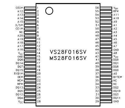 Specifications
Temperature Under Bias
-SE1..........-55 to a125
-SE2 ..........-40to a125
Storage Temperature..-65 to a125
NOTICE: This data sheet contains information on products in the sampling and initial production phases of development. The specifications are subject to change without notice. Verify with your local Intel Sales office that you have the latest data sheet before finalizing a design.
*WARNING: Stressing the device beyond the "Absolute Maximum Ratings'' may cause permanent damage. These are stress ratings only. Operation beyond the "Operating Conditions'' is not recommended and extended exposure beyond the "Operating Conditions'' may affect device reliability.
DescriptionThe VS/MS28F016SV is a high-performance, 16-Mbit (16,777,216-bit) block erasable, non-volatile random access memory, organized as either 1 Mword x 16 or 2 Mbyte x 8. The VS/MS28F016SV includes thirty-two 64-KB (65,536 byte) blocks or thirty-two 32-KW (32,768 word) blocks. A chip memory map is shown in Figure 3.
The implementation of a new architecture, with many enhanced features, will improve the device operating characteristics and result in greater product reliability and ease of use.
The VS/MS28F016SV incorporates SmartVoltage technology, providing VCC operation at both 3.3V and 5.0V and program and erase capability at VPP e 12.0V or 5.0V. Operating at VCC e 3.3V, the VS/MS28F016SV consumes approximately one-half the power consumption at 5.0V VCC, while 5.0V VCC provides highest read performance capability. VPP e 5.0V operation eliminates the need for a separate 12.0V converter, while VPP e 12.0V maximizes write/erase performance. In addition to the flexible program and erase voltages, the dedicated VPP gives complete code protection with VPP VPPLK.
Depending on system design specifications, the VS/MS28F016SV is capable of supporting
-80 ns access times with a VCC of 5.0V g5% and loading of 30 pF
-85 ns access times with a VCC of 5.0V g10% and loading of 100 pF
-120 ns access times with a VCC of 3.3V g5% and loading of 50 pF
A 3/5# input pin configures the device's internal circuitry for optimal 3.3V or 5.0V Read/Write operation.
A Command User Interface (CUI) serves as the system interface between the microprocessor or microcontroller and the internal memory operation.
Internal Algorithm Automation allows Byte/Word Writes and Block Erase operations to be executed using a Two-Write command sequence to the CUI in the same way as the VE28F008 or M28F008 8-Mbit FlashFile memory.
A super-set of commands has been added to the basic VE28F008 or M28F008 command-set to achieve higher write performance and provide additional capabilities. These new commands and features include:
`Page Buffer Writes to Flash
`Command Queuing Capability
`Automatic Data Writes during Erase
`Software Locking of Memory Blocks
`Two-Byte Successive Writes in 8-bit Systems
`Erase All Unlocked Blocks

 VS28F016SV Data Sheet


