V54C316162V

Features: JEDEC Standard 3.3V Power SupplyThe V54C316162V is ideally suited for high performance graphics peripheral applicationsSingle Pulsed RAS InterfaceProgrammable CAS Latency: 2, 3All Inputs are sampled at the positive going edge of clockProgrammable Wrap Sequence: Sequential or InterleavePr...

product image

V54C316162V Picture
SeekIC No. : 004539956 Detail

V54C316162V: Features: JEDEC Standard 3.3V Power SupplyThe V54C316162V is ideally suited for high performance graphics peripheral applicationsSingle Pulsed RAS InterfaceProgrammable CAS Latency: 2, 3All Inputs a...

floor Price/Ceiling Price

Part Number:
V54C316162V
Supply Ability:
5000

Price Break

  • Qty
  • 1~5000
  • Unit Price
  • Negotiable
  • Processing time
  • 15 Days
Total Cost: $ 0.00

SeekIC Buyer Protection PLUS - newly updated for 2013!

  • Escrow Protection.
  • Guaranteed refunds.
  • Secure payments.
  • Learn more >>

Month Sales

268 Transactions

Rating

evaluate  (4.8 stars)

Upload time: 2024/11/21

Payment Methods

All payment methods are secure and covered by SeekIC Buyer Protection PLUS.

Notice: When you place an order, your payment is made to SeekIC and not to your seller. SeekIC only pays the seller after confirming you have received your order. We will also never share your payment details with your seller.
Product Details

Description


Features:

 JEDEC Standard 3.3V Power Supply
 The V54C316162V is ideally suited for high performance graphics peripheral applications
 Single Pulsed RAS Interface
 Programmable CAS Latency: 2, 3
 All Inputs are sampled at the positive going edge of clock
 Programmable Wrap Sequence: Sequential or Interleave
 Programmable Burst Length: 1, 2, 4, 8 and Full Page for Sequential and 1, 2, 4, 8 for Interleave
 UDQM & LDQM for byte masking
 Auto & Self Refresh
 4K Refresh Cycles/64 ms
 Burst Read with Single Write Operation


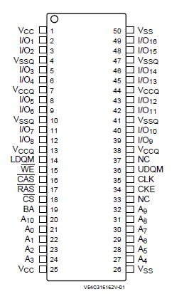
Pinout

  Connection Diagram


Specifications

Operating temperature range .............................................0 to 70 °C
Storage temperature range .......................................... -55 to 150 °C
Input/output voltage ........................................... -0.3 to (VCC+0.3) V
Power supply voltage ..................................................... -0.3 to 4.6 V
Power dissipation ......................................................................... 1 W
Data out current (short circuit) .................................................. 50 mA


Description

The V54C316162V is a 16,777,216 bits synchronous high data rate DRAM organized as 2 x 524,288 words by 16 bits. The device is designed to comply with JEDEC standards set for synchronous DRAM products, both electrically and mechanically. Synchronous design allows precise cycle control with the system clock. The CAS latency, burst length and burst sequence must be programmed into device prior to access operation.


Customers Who Bought This Item Also Bought

Margin,quality,low-cost products with low minimum orders. Secure your online payments with SeekIC Buyer Protection.
Static Control, ESD, Clean Room Products
Optoelectronics
Inductors, Coils, Chokes
Line Protection, Backups
Test Equipment
View more