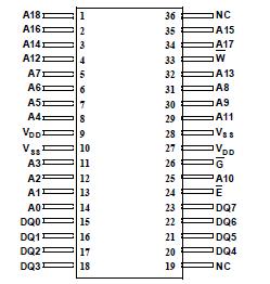
Features: · 100ns (5 volt supply) maximum address access time· Asynchronous operation for compatibility with industrystandard 512K x 8 SRAMs· TTL compatible inputs and output levels, three-state bidirectional data bus· Typical radiation performance- Total dose: 30krad(Si)- 30krad(Si) to 300krad(Si...
UT7Q512: Features: · 100ns (5 volt supply) maximum address access time· Asynchronous operation for compatibility with industrystandard 512K x 8 SRAMs· TTL compatible inputs and output levels, three-state bid...
SeekIC Buyer Protection PLUS - newly updated for 2013!
268 Transactions
All payment methods are secure and covered by SeekIC Buyer Protection PLUS.
SYMBOL | PARAMETER |
LIMITS |
UNIT |
VDD | DC supply voltage |
-0.3 to +7.0 |
V |
VI/O | Voltage on any pin |
-0.5 to 7.0V |
V |
II | DC input current |
±10 |
mA |
TSTG | Storage temperature |
-65 to +150 |
°C |
PD | Maximum power dissipation |
1 |
mW |
TJ | Maximum junction temperature |
+150 |
°C |
QJC | Thermal resistance, junction-to-case |
10 |
°C/W |
Note:
1. Stresses outside the listed absolute maximum ratings may cause permanent damage to the device. This is a stress rating only, and functional operation of the device at these or any other conditions beyond limits indicated in the operational sections of this specification is not recommended. Exposure to absolute maximum rating conditions for extended periods may affect device reliability.
2. Maximum junction temperature may be increased to +175°C during burn-in and steady-static life.
3. Test per MIL-STD-883, Method 1012.
The QCOTSTM UT7Q512 Quantified Commercial Off-the- Shelf product is a high-performance CMOS static RAM organized as 524,288 words by 8 bits. Easy memory expansion is provided by an active LOW Chip Enable (E), an active LOW Output Enable (G), and three-state drivers. This device has a power-down feature that reduces power consumption by more than 90% when deselected.
Writing to the UT7Q512 is accomplished by taking the Chip Enable One (E) input LOW and the Write Enable (W) input LOW. Data on the eight I/O pins (DQ0 through DQ7) is then written into the location specified on the address pins (A0 through A18). Reading from the device is accomplished by taking Chip Enable One (E) and Output Enable (G) LOW while forcing Write Enable (W) HIGH. Under these conditions, the contents of the memory location specified by the address pins will appear on the eight I/O pins.
The eight input/output pins (DQ0 through DQ7) are placed in a high impedance state when the device is deselected (E, HIGH), the outputs are disabled (G HIGH), or during a write operation (E LOW and W LOW).