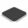
Features: The uPSD325X devices combine a Flash PSD architecture with an 8032 microcontroller core. The uPSD325X devices of Flash PSDs feature dual banks of Flash memory, SRAM, general purpose I/O and programmable logic, supervisory functions and access via USB, I2C, ADC, DDC and PWM channels, and an on-board 8032 microcontroller core, with two UARTs, three 16-bit Timer/Counters and two External Interrupts. As with other Flash PSD families, the uPSD325X devices are also in-system programmable (ISP) via a JTAG ISP interface.
Large 32KByte SRAM with battery back-up option
Dual bank Flash memories
128KByte or 256KByte main Flash memory
32KByte secondary Flash memory
Content Security
Block access to Flash memory
Programmable Decode PLD for flexible address mapping of all memories within 8032 space.
High-speed clock standard 8032 core (12-cycle)
USB Interface (some devices only)
I2C interface for peripheral connections
5 Pulse Width Modulator (PWM) channels
Analog-to-Digital Converter (ADC)
Standalone Display Data Channel (DDC)
Six I/O ports with up to 46 I/O pins
3000 gate PLD with 16 macrocells
Supervisor functions with Watchdog Timer
In-System Programming (ISP) via JTAG
Zero-Power Technology
Single Supply Voltage
4.5 to 5.5V
3.0 to 3.6VPinout Specifications
| Symbol |
Parameter |
Min. |
Max. |
Unit |
| TSTG |
Storage Temperature |
65 |
125 |
|
| TLEAD |
Lead Temperature during Soldering (20 seconds max.)(1) |
|
235 |
|
| VIO |
Input and Output Voltage (Q = VOH or Hi-Z) |
0.5 |
6.5 |
V |
| VCC |
Supply Voltage |
0.5 |
6.5 |
V |
| VPP |
Device Programmer Supply Voltage |
0.5 |
14.0 |
V |
| VESD |
Electrostatic Discharge Voltage (Human Body Model) 2 |
2000 |
2000 |
V |
Description UPSD3254BV Dual bank Flash memories
Concurrent operation, read from memory while erasing and writing the other. In-Application Programming (IAP) for remote updates
Large 128KByte or 256KByte main Flash memory for application code, operating systems, or bit maps for graphic user interfaces
Large 32KByte secondary Flash memory divided in small sectors. Eliminate external EEPROM with software EEPROM emulation
Secondary Flash memory is large enough for sophisticated communication protocol (USB) during IAP while continuing critical system tasks
UPSD3254BV Large SRAM with battery back-up option
32KByte SRAM for RTOS, high-level languages, communication buffers, and stacks
UPSD3254BV Programmable Decode PLD for flexible address mapping of all memories
Place individual Flash and SRAM sectors on any address boundary
Built-in page register breaks restrictive 8032 limit of 64KByte address space
Special register swaps Flash memory segments between 8032 "program" space and "data" space for efficient In-Application Programming
UPSD3254BV High-speed clock standard 8032 core (12-cycle)
40MHz operation at 5V, 24MHz at 3.3V
2 UARTs with independent baud rate, three 16-bit Timer/Counters and two External Interrupts
UPSD3254BV USB Interface (some devices only)
Supports USB 1.1 Slow Mode (1.5Mbit/s)
Control endpoint 0 and interrupt endpoints 1 and 2
UPSD3254BV I
2C interface for peripheral connections
Capable of master or slave operation
UPSD3254BV 5 Pulse Width Modulator (PWM) channels
Four 8-bit PWM units
One 8-bit PWM unit with programmable period
UPSD3254BV 4-channel, 8-bit Analog-to-Digital Converter (ADC) with analog supply voltage (VREF)
UPSD3254BV Standalone Display Data Channel (DDC)
For use in monitor, projector, and TV applications
Compliant with VESA standards DDC1 and DDC2B
Eliminate external DDC PROM
UPSD3254BV Six I/O ports with up to 46 I/O pins
Multifunction I/O: GPIO, DDC, I
2C, PWM, PLD I/O, supervisor, and JTAG
Eliminates need for external latches and logic
UPSD3254BV 3000 gate PLD with 16 macrocells
Create glue logic, state machines, delays,etc.
Eliminate external PALs, PLDs, and 74HCxx
Simple PSDsoft Express software...Free
UPSD3254BV Supervisor functions
Generates reset upon low voltage or watchdog time-out. Eliminate external supervisor device
RESET Input pin; Reset output via PLD
UPSD3254BV In-System Programming (ISP) via JTAG
Program entire chip in 10 - 25 seconds with no involvement of 8032
Allows efficient manufacturing, easy product testing, and Just-In-Time inventory
Eliminate sockets and pre-programmed parts
Program with FlashLINK
TM cable and any PC
UPSD3254BV Content Security
Programmable Security Bit blocks access of device programmers and readers
UPSD3254BV Zero-Power Technology
Memories and PLD automatically reach standby current between input changes
UPSD3254BV Packages
52-pin TQFP
80-pin TQFP: allows access to 8032 address/data/control signals for connecting to external peripherals

 UPSD3254BV Data Sheet


