UPD178004

Features: • Internal high-capacity ROM and RAM • Instruction Cycle: 0.44 ms (4.5-MHz crystal oscillator used)• Large array of on-chip peripheral hardware General-purpose input/output port, A/D converter, serial interface, timer, frequency counter, power-ON clear circuits.• ...

product image

UPD178004 Picture
SeekIC No. : 004538100 Detail

UPD178004: Features: • Internal high-capacity ROM and RAM • Instruction Cycle: 0.44 ms (4.5-MHz crystal oscillator used)• Large array of on-chip peripheral hardware General-purpose input/outp...

floor Price/Ceiling Price

Part Number:
UPD178004
Supply Ability:
5000

Price Break

  • Qty
  • 1~5000
  • Unit Price
  • Negotiable
  • Processing time
  • 15 Days
Total Cost: $ 0.00

SeekIC Buyer Protection PLUS - newly updated for 2013!

  • Escrow Protection.
  • Guaranteed refunds.
  • Secure payments.
  • Learn more >>

Month Sales

268 Transactions

Rating

evaluate  (4.8 stars)

Upload time: 2024/11/22

Payment Methods

All payment methods are secure and covered by SeekIC Buyer Protection PLUS.

Notice: When you place an order, your payment is made to SeekIC and not to your seller. SeekIC only pays the seller after confirming you have received your order. We will also never share your payment details with your seller.
Product Details

Description


Features:

• Internal high-capacity ROM and RAM
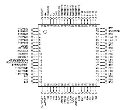
     Connection Diagram
• Instruction Cycle: 0.44 ms (4.5-MHz crystal oscillator used)
• Large array of on-chip peripheral hardware General-purpose input/output port, A/D converter, serial interface, timer, frequency counter, power-ON clear circuits.
• On-chip hardware for a PLL frequency synthesizer. Dual modulus pre-scaler, programmable divider, phase comparator, charge pump.
• Vector Interrupts: 17
• Supply Voltage: VDD = 4.5 to 5.5 V (during PLL operation)
                            VDD = 3.5 to 5.5 V (during CPU operation, when the system clock is fX/2 or lower)
                            VDD = 4.5 to 5.5 V (during CPU operation, when the system clock is fX)


Application

Car stereo, home stereo systems.


Pinout

  Connection Diagram


Specifications

Parameter Symbol Test Conditions Rating Unit
Power supply voltage VDD   -0.3 to +7.0
V
Input voltage VI1 Excluding P60 to P63 0.3 ~ VDD+0.3 V
V12

P60 to P63

N-ch Open-drain 0.3 ~ VDD+16 V
Output voltage VO   0.3 ~ VDD+0.3 V
Output withstand voltage VBDS P132 to P134 N-ch Open-drain 16 V
Analog input voltage VAN P10 to P15 Analog input pin 0.3 to VDD + 0.3 V
Output current high IOH 1 pin 10 mA

P01 to P06, P30 to P37, P56, P57, P60 to P67,P120 to P125 total

15 mA
P10 to P15, P20 to P27, P40 to P47, P50 to P55,P132 to P134 total 15 mA
Output current low IOL Note 1 pin Peak value 15 mA
Effective value 7.5 mA

Operating ambient

temperature

TA   40 to +85 °C
Storage temperature Tstg   40 to +85 °C


Customers Who Bought This Item Also Bought

Margin,quality,low-cost products with low minimum orders. Secure your online payments with SeekIC Buyer Protection.
Audio Products
Integrated Circuits (ICs)
Memory Cards, Modules
Isolators
Programmers, Development Systems
Static Control, ESD, Clean Room Products
View more