UPD16856

Features: • Supply voltage for controller block: 5 V, supply voltage for output block: 12 V3 V input available for the input interface• Low on-state resistance (total on-state resistance of upper and lower MOS FETs) RON = 1.3 Ω (TYP.)• Low power consumption due to 3-phase f...

product image

UPD16856 Picture
SeekIC No. : 004538083 Detail

UPD16856: Features: • Supply voltage for controller block: 5 V, supply voltage for output block: 12 V3 V input available for the input interface• Low on-state resistance (total on-state resistance...

floor Price/Ceiling Price

Part Number:
UPD16856
Supply Ability:
5000

Price Break

  • Qty
  • 1~5000
  • Unit Price
  • Negotiable
  • Processing time
  • 15 Days
Total Cost: $ 0.00

SeekIC Buyer Protection PLUS - newly updated for 2013!

  • Escrow Protection.
  • Guaranteed refunds.
  • Secure payments.
  • Learn more >>

Month Sales

268 Transactions

Rating

evaluate  (4.8 stars)

Upload time: 2025/1/4

Payment Methods

All payment methods are secure and covered by SeekIC Buyer Protection PLUS.

Notice: When you place an order, your payment is made to SeekIC and not to your seller. SeekIC only pays the seller after confirming you have received your order. We will also never share your payment details with your seller.
Product Details

Description


Features:

• Supply voltage for controller block: 5 V, supply voltage for output block: 12 V3 V input available for the input interface
• Low on-state resistance (total on-state resistance of upper and lower MOS FETs) RON = 1.3 Ω  (TYP.)
• Low power consumption due to 3-phase full-wave PWM drive method
• On-chip hole bias switch (linked with STB pin)
• On-chip IND (FG) pulse switching function, 1-phase output or 3-phase composite output
• START/STOP pin included, acting as a brake during STOP
• Standby pins included, turning off internal circuit in standby
• Low current consumption: IDD = 3 mA (Max.), IDD (ST) = 1 µA (Max.)
• On-chip thermal shutdown circuit
• On-chip current limiting circuit; reference voltage can be set externally
• On-chip low voltage malfunction prevention circuit
• On-chip reverse rotation prevention circuit 
• 30-pin plastic shrink SOP (300 mil)


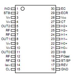
Pinout

  Connection Diagram


Specifications

Parameter

 Symbol

Conditions

Ratings

Unit

Supply voltage

VDD


−0.5 to +6.0

V

VM


−0.5 to +13.5

V

Input voltage

VIN


−0.5 to VDD + 0.5

V

Instantaneous output current
Note 1

IDR (pulse)

PW 5 ms, Duty 30%

±2.0

A/phase

Power consumptionNote 2

PT


1.0

W

Peak channel temperature

TCH (MAX)


150

Storage temperature range

Tstg


−55 to +150


Customers Who Bought This Item Also Bought

Margin,quality,low-cost products with low minimum orders. Secure your online payments with SeekIC Buyer Protection.
Audio Products
Transformers
Inductors, Coils, Chokes
Optoelectronics
Cables, Wires - Management
RF and RFID
View more