UCD9501

Features: •High-Performance Static CMOS Technology100 MHz (10-nsCycleTime)Low-Power (1.8-VCore,3.3-VI/O) Design3.3-V Flash Voltage•JTAG Boundary Scan Support•High-Performance 32-BitCPU (TMS320C28x)16x16 and 32x32 MAC Operations16x16 Dual MACHarvard Bus ArchitectureAtomic Operatio...

product image

UCD9501 Picture
SeekIC No. : 004536189 Detail

UCD9501: Features: •High-Performance Static CMOS Technology100 MHz (10-nsCycleTime)Low-Power (1.8-VCore,3.3-VI/O) Design3.3-V Flash Voltage•JTAG Boundary Scan Support•High-Performance 32-Bi...

floor Price/Ceiling Price

Part Number:
UCD9501
Supply Ability:
5000

Price Break

  • Qty
  • 1~5000
  • Unit Price
  • Negotiable
  • Processing time
  • 15 Days
Total Cost: $ 0.00

SeekIC Buyer Protection PLUS - newly updated for 2013!

  • Escrow Protection.
  • Guaranteed refunds.
  • Secure payments.
  • Learn more >>

Month Sales

268 Transactions

Rating

evaluate  (4.8 stars)

Upload time: 2025/1/6

Payment Methods

All payment methods are secure and covered by SeekIC Buyer Protection PLUS.

Notice: When you place an order, your payment is made to SeekIC and not to your seller. SeekIC only pays the seller after confirming you have received your order. We will also never share your payment details with your seller.
Product Details

Description


Features:

•High-Performance Static CMOS Technology
100 MHz (10-nsCycleTime)
Low-Power (1.8-VCore,3.3-VI/O) Design
3.3-V Flash Voltage
•JTAG Boundary Scan Support
•High-Performance 32-BitCPU (TMS320C28x)
16x16 and 32x32 MAC Operations
16x16 Dual MAC
Harvard Bus Architecture
Atomic Operations
Fast Interrupt Response and Processing
Unified Memory Programming Model
Code-Efficient(inC/C++and Assembly)
•On-Chip Memory
F2808:64K X 16 Flash,18K X 16 SARAM
  F2806:32K X 16 Flash,10K X 16 SARAM
  F2801:16K X 16 Flash,6K X 16 SARAM
  9501:16K X 16 Flash,6K X 16 SARAM
1K x 16 OTP ROM
•Boot ROM (4Kx16)
With Software Boot Modes (viaSCI,SPI,CAN,I2C,and Parallel I/O)
Standard Math Tables
•Clock and System Control
Dynamic PLL Ratio Changes Supported
On-Chip Oscillator
Clock-Fail-Detect Mode
Watchdog Timer Module
•Any GPIO A Pin Can Be Connected to One of the Three External Core Interrupts
•Peripheral Interrupt Expansion (PIE) Block That Supports All 43 Peripheral Interrupts
•128-Bit Security Key/Lock
Protects Flash/OTP/L0/L1 Blocks
Prevents Firmware Reverse Engineering
•Enhanced Control Peripherals
Up to 16 PWM Outputs
Up to 4 HRPWM Outputs With 150 ps MEP Resolution
Up to Four Capture Inputs
Up to Two Quadrature Encoder Interfaces
Up to Six 32-bit Timers
Up to Six 16-bit Timers
•Three 32-Bit CPU Timers
•Serial Port Peripherals
Up to 4 Serial Peripheral Interface(SPI) Modules
Up to 2 Serial Communications Interface (SCI),Standard UART Modules
Up to 2 Enhanced Controller Area Network(eCAN) Modules
One Inter-Integrated-Circuit(I2C) Bus
•12-Bit ADC,16 Channels
2 x 8 Channel Input Multiplexer
Two Sample-and-Hold
Single/Simultaneous Conversions
Fast Conversion Rate:160ns/6.25 MSPS
Internal or External Reference
•Up to 35 Individually Programmable,
  Multiplexed General-Purpose Input/Output
  (GPIO) Pins With Input Filtering
•Advanced Emulation Features
Analysis and Breakpoint Functions
Real-Time Debug via Hardware
•Developmen tTools Include
ANSIC/C++Compiler/Assembler/Linker
Supports TMS320C24 x ™/240x Instructions
Code Composer Studio™IDE
DSP/BIOS™
JTAG Scan Controllers(1)[Texas Instruments(TI)orThird-Party]
Evaluation Modules
Broad Third-Party Digital Motor Control Support
•Low-PowerModesandPowerSavings
IDLE,STANDBY,HALTModesSupported
Disable Individual Peripheral Clocks
•Package Options
Thin Quad Flatpack(PZ)
MicroStar BGA™(GGM,ZGM)
•Temperature Options:
A:-40°Cto85°C(PZ,GGM,ZGM)
S:-40°Cto125°C(PZ,GGM,ZGM)
Q:-40°Cto125°C(PZ)


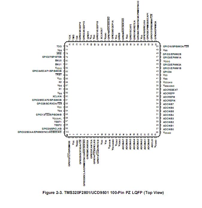
Pinout

  Connection Diagram


Specifications

Supply voltage range,VDDIO,VDD3VFL

with respect toVSS

-0.3Vto4.6V

Supply voltage range,VDDA2,VDDAIO

with respect toVSSA

-0.3Vto4.6V

Supply voltage range,VDD

with respect toVSS

-0.3Vto2.5V

Supplyvoltagerange,VDD1A18,VDD2A18

with respect toVSSA

-0.3Vto2.5V

Supply voltagerange,VSSA2,VSSAIO,VSS1AGND,VSS2AGND

with respect toVSS

-0.3Vto0.3V

Input voltage range,VIN

-0.3Vto4.6V

Output voltage range,VO

-0.3Vto4.6V

Inputclampcurrent,IIK(VIN<0orVIN>VDDIO)(3)

±20mA

Output clamp current,IOK(VO<0orVO>VDDIO)

±20mA

Operating ambient temper atureranges,

TA:Aversion(GGM,PZ)(4)

-40°Cto85°C

TA:Sversion(GGM,PZ)(4)

-40°Cto125°C

TA:Qversion(PZ)(4)

-40°Cto125°C

Junction temperatu rerange,Tj(4)

-40°Cto150°C

Storage temperature range,Tstg(4)

-65°Cto150°C


Customers Who Bought This Item Also Bought

Margin,quality,low-cost products with low minimum orders. Secure your online payments with SeekIC Buyer Protection.
Programmers, Development Systems
Prototyping Products
DE1
Circuit Protection
Industrial Controls, Meters
Batteries, Chargers, Holders
View more