UCC3776

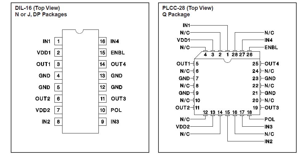
Features: • High Peak Output Current Each Output 1.5A Source, 2.0A Sink• Wide Operating Voltage Range 4.5V to 18V• Thermal Shutdown• CMOS Compatible Inputs• Outputs Are Active Low for Undervoltage Lockout ConditionPinoutSpecificationsInput Supply Voltage, VDD1, VDD2 ...

product image

UCC3776 Picture
SeekIC No. : 004535975 Detail

UCC3776: Features: • High Peak Output Current Each Output 1.5A Source, 2.0A Sink• Wide Operating Voltage Range 4.5V to 18V• Thermal Shutdown• CMOS Compatible Inputs• Outputs Ar...

floor Price/Ceiling Price

Part Number:
UCC3776
Supply Ability:
5000

Price Break

  • Qty
  • 1~5000
  • Unit Price
  • Negotiable
  • Processing time
  • 15 Days
Total Cost: $ 0.00

SeekIC Buyer Protection PLUS - newly updated for 2013!

  • Escrow Protection.
  • Guaranteed refunds.
  • Secure payments.
  • Learn more >>

Month Sales

268 Transactions

Rating

evaluate  (4.8 stars)

Upload time: 2025/1/6

Payment Methods

All payment methods are secure and covered by SeekIC Buyer Protection PLUS.

Notice: When you place an order, your payment is made to SeekIC and not to your seller. SeekIC only pays the seller after confirming you have received your order. We will also never share your payment details with your seller.
Product Details

Description


Features:

• High Peak Output Current Each Output 1.5A Source, 2.0A Sink
• Wide Operating Voltage Range 4.5V to 18V
• Thermal Shutdown
• CMOS Compatible Inputs
• Outputs Are Active Low for Undervoltage Lockout Condition


Pinout

  Connection Diagram


Specifications

Input Supply Voltage, VDD1, VDD2 . . . . . . . . . . . . . . . . . . . . . . . . . . . . . . . . . . . . .20V
Maximum DC Voltage Difference, VDD1 vs.VDD2 . . . . . . .. . . . . . . . . . . . . . . . . .100mV
Logic Input, IN1, IN4, ENBL
Maximum forced voltage . . . . . . . . . . . . . . . . . . . . . . . . . . .. .  . . .-0.3 to VDD1 + 0.3V
Logic Inputs, IN2, IN3, POL
Maximum forced voltage . . . . . . . . . . . . . . . . . . . . . . . . . . . . . . . .-0.3 to VDD2 + 0.3V
Latch-up Protection withstand Reverse Current
IREV, OUT1, OUT2, OUT3, OUT4 . . . . . . . . . . . . . . . . . . . . . . . . . . . .. . . .  . . . . .500mA
Power Outputs, OUT1, OUT2, OUT3, OUT4
Maximum pulsed current (10% duty max, 10msec max pulse width) . . . . . . . . . . . .3A
Storage Temperature . . . . . . . . . . . . . . . . . . . . . . . . . . . . . . . .  . . . . .-65 to +150
Operating Junction Temperature . . . . . . . . . . . . . . . . . . . . . . . . . . . . .-55 to +150
Lead Temperature (Soldering, 10 Seconds) . . . . . . . . . . . . . . . . . . . . . . . . . . . . .300

All currents are positive into, negative out of the specified terminal. Consult Packaging Section of Databook for thermal limitations and considerations of packages.


Description

The UCC3776 is a four output BCDMOS buffer/driver designed to drive highly capacitive loads such as power MOSFET gates at high speeds. The device can be configured as either an inverting or non-inverting driver via the POL pin. The outputs are enabled by ENBL. When disabled, all outputs are active low. The device incorporates thermal shutdown with hysteresis for stability. The device also includes an undervoltage lockout circuit (UVLO) with hysteresis which disables the outputs when VDD is below a preset threshold. The outputs are held low during undervoltage lockout, even in the absence of VDD power to the device. This helps prevent MOSFET turn-on due to capacitive current through the gate-drain capacitance of the power MOSFET in the presence of high dV/dts. The logic input thresholds are compatible with standard 5V HCMOS logic.


Customers Who Bought This Item Also Bought

Margin,quality,low-cost products with low minimum orders. Secure your online payments with SeekIC Buyer Protection.
Integrated Circuits (ICs)
Soldering, Desoldering, Rework Products
Computers, Office - Components, Accessories
View more