Features: • 1V Input Voltage Operation Startup Guaranteed Under Full Load on Main Output With Operation Down to 0.4V
• Input Voltage Range of 1V to VOUT + 0.5V
• 500mW Output Power at Battery Voltages as Low as 0.8V
• Secondary 9V Supply From a Single Inductor
• Adjustable Output Power Limit Control
• Output Fully Disconnected in Shutdown
• Adaptive Current Mode Control for Optimum Efficiency
• 8A Shutdown Supply Current
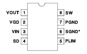
Pinout Specifications
VIN Voltage . . . . . . . . . . . . . . . . . . . . . . . . . . . . . . 0.3V to 10V
SD Voltage . . . . . . . . . . . . . . . . . . . . . . . . . . . . . . 0.3V to V IN
PLIM Voltage. . . . . . . . . . . . . . . . . . . . . . . . . . . . . 0.3V to 10V
VGD Voltage . . . . . . . . . . . . . . . . . . . . . . . . . . . . . 0.3V to 15V
SW Voltage . . . . . . . . . . . . . . . . . . . . . . . . . . . . . . 0.3V to 15V
VOUT Voltage . . . . . . . . . . . . . . . . . . . . . . . . . . . . 0.3V to 10V
Storage Temperature . . . . . . . . . . . . . . . .. . 65°C to +150°C
Junction Temperature. . . . . . . . . . . . . . . . . . 55°C to +150°C
Lead Temperature (Soldering, 10 sec.) . . . . . . . . . . . . . +300°C
Currents are positive into, negative out of the specified terminal. Consult Packaging Section of Databook for thermal limitations and considerations of packages.
DescriptionThe UCC3941 family of low input voltage single inductor boost converters are optimized to operate from a single or dual alkaline cell, and step up to a 3.3V, 5V, or an adjustable output at 500mW. The UCC3941 family also provides an auxiliary 9V 100mW output, primarily for the gate drive supply, which can be used for applications requiring an auxiliary output such as a 5V supply by linear regulating. The primary output will start up under full load at input voltages typically as low as 0.8V, with a guaranteed maximum of 1V, and will operate down to 0.4V once the converter is operating, maximizing battery utilization.
Demanding applications such as Pagers and PDA's require high efficiency from several milli-watts to several hundred milli-watts, and the UCC3941 family accommodates these applications with >80% typical efficiencies over the wide range of operation. The high efficiency at low output current is achieved by optimizing switching and conduction losses along with low quiescent current. At higher output current the 0.25switch, and 0.4synchronous rectifier, along with continuous mode conduction, provide high efficiency. The wide input voltage range on the UCC3941 family can accommodate other power sources such as NiCd and NiMH.
Other features include maximum power control and shutdown control. Packages available are the 8-pin SOIC (D) and 8-pin DIP (N or J).

 UCC2941-3 Data Sheet


