UCC28528

Features: ·Provides Control of PFC and PWM Power Stages In One Device·Trailing-Edge PFC, Trailing-Edge PWM Modulation·Built-In Sequencing of PFC and PWM Turn-On·2-A Source and 3-A Sink Gate Drive for Both PFC and PWM Stages·Typical 16-ns Rise Time and 7-ns Fall Time into 1-nF Loads PFC Features...

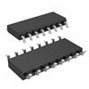
product image

UCC28528 Picture
SeekIC No. : 004535906 Detail

UCC28528: Features: ·Provides Control of PFC and PWM Power Stages In One Device·Trailing-Edge PFC, Trailing-Edge PWM Modulation·Built-In Sequencing of PFC and PWM Turn-On·2-A Source and 3-A Sink Gate Drive fo...

floor Price/Ceiling Price

Part Number:
UCC28528
Supply Ability:
5000

Price Break

  • Qty
  • 1~5000
  • Unit Price
  • Negotiable
  • Processing time
  • 15 Days
Total Cost: $ 0.00

SeekIC Buyer Protection PLUS - newly updated for 2013!

  • Escrow Protection.
  • Guaranteed refunds.
  • Secure payments.
  • Learn more >>

Month Sales

268 Transactions

Rating

evaluate  (4.8 stars)

Upload time: 2025/1/6

Payment Methods

All payment methods are secure and covered by SeekIC Buyer Protection PLUS.

Notice: When you place an order, your payment is made to SeekIC and not to your seller. SeekIC only pays the seller after confirming you have received your order. We will also never share your payment details with your seller.
Product Details

Description


Features:

·Provides Control of PFC and PWM Power Stages In One Device
·Trailing-Edge PFC, Trailing-Edge PWM Modulation
·Built-In Sequencing of PFC and PWM Turn-On
·2-A Source and 3-A Sink Gate Drive for Both PFC and PWM Stages
·Typical 16-ns Rise Time and 7-ns Fall Time into 1-nF Loads PFC Features
− Average-Current-Mode Control for Continuous Conduction Mode Operation
− Highly-Linear Multiplier for Near-Unity Power Factor
− Input Voltage Feedforward Implementation
− Improved Load Transient Response
− Accurate Power Limiting
− Zero Power Detect
   PWM Features
− Peak-Current-Mode Control Operation
− 1:1 PFC:PWM Frequency Option
− Programmable maximum Duty Cycle Limit Up to 90%
− Programmable Soft-Start


Application

·High-Efficiency Server and DesktopSupplies
·High-Efficiency Telecom AC-DC Converter


Specifications

over operating free-air temperature (unless otherwise noted)†  Connection Diagram
Supply voltage VCC
Idle . . . . . . . . . . . . . . . . . . . . . . . . . . . . . . . . . . . . . . . . . . . . . . . . . . . . . . . . . ... . . 20 V
Operating . . . . . . . . . . . . . . . . . . . . . . . . . . . . . . . . . . . . . . . . . . . . . . . . . . . . . . . . 18 V
Gate drive current (GT1, GT2)
Continuous . . . . . . . . . . . . . . . . . . . . . . . . . . . . . . . . . . . . . . . . . . . . . . . . . .   . .. . 0.4 A
Pulsed
Sourcing . . . . . . . . . . . . . . . . . . . . . . . . . . . . . . . . . . . . . . . . . . . . . . . . . . . . .. . . −2.5 A
Sinking . . . . . . . . . . . . . . . . . . . . . . . . . . . . . . . . . . . . . . . . . . . . . . . . . . . . . .  . .. . 3.5 A
Maximum GT1, GT2 voltage . . . . . . . . . . . . . . . . . . . . . . . . . . . . .  . −0.5 V to VCC+0.3 V
Input voltage
VSENSE . . . . . . . . . . . . . . . . . . . . . . . . . . . . . . . . . . . . . . . . . . . . . . . . . . . . . 0 V to 11 V
D_MAX, SS2, CAOUT, ISENSE1, MOUT, VFF . . . . . . . . . . . . . . . . .  .−0.5 V to VREF+0.3 V
VAOUT, CT_BUFF, ISENSE2, PKLMT . . . . . . . . . . . . . . . . . . . . . . . . . . . . . .. −0.5 V to 6 V
Pin Current
RT . . . . . . . . . . . . . . . . . . . . . . . . . . . . . . . . . . . . . . . . . . . . . . . . . . . . . .   . . .. . −0.5 mA
VFF . . . . . . . . . . . . . . . . . . . . . . . . . . . . . . . . . . . . . . . . . . . . . . . . . . . . . . . . . .   . −5 mA
CT_BUFF . . . . . . . . . . . . . . . . . . . . . . . . . . . . . . . . . . . . . . . . . . . . . . . . . . . . . .  . .  1 mA
VAOUT, VERR, ISENSE2, SS2, CAOUT, IAC . . . . . . . . . . . . . . . . . . . . . . . . .  . . . . .. 10 mA
Maximum pin capacitance
ISENSE2 . . . . . . . . . . . . . . . . . . . . . . . . . . . . . . . . . . . . . . . . . . . . .  . . . . . . . . . .  220 pF
Operating junction temperature range, TJ . . . . . . . . . . . . . . . . . . . . . . . −55 to 150
Storage temperature range, Tstg . . . . . . . . . . . . . . . . . . . . . . . . . . . . .. −65 to 150
Lead temperature 1.6mm (1/16 inch from case for 10 seconds) . . . . . . . . . . . .  .. 300

† Stresses beyond those listed under "absolute maximum ratings" may cause permanent damage to the device. These are stress ratings only, and functional operation of the device at these or any other conditions beyond those indicated under recommended operating conditions is not implied.

Exposure to absolute−maximum−rated conditions for extended periods may affect reliability.

‡ Currents are positive into, negative out of the specified terminal. All voltages are referenced to GND.


Description

The UCC28521 and UCC28528 combination PFC/PWM controllers provide complete control functionality for any off-line power system requiring compliance with the IEC1000−3−2 harmonic reduction requirements. By combining the control and drive signals for the PFC and the PWM stages into a single device, significant performance and cost benefits are gained.

Based on the UCC28511, the new devices employ an average current mode control architecture with input voltage feedforward. The major difference of the UCC28521/28 is the trailing-edge /trailing-edge (TEM/TEM) modulation scheme for the PFC/PWM stages. The UCC28528 differs from the UCC28521 as its PWM stage does not turn off with the falling bulk voltage. The UCC28528 PWM was designed for low power auxiliary supplies.

These devices offer performance advantages over earlier generation combination controllers. A key PWM feature is programmable maximum duty cycle. For the PFC stage, the devices feature an improved multiplier and the use of a transconductance amplifier for enhanced transient response.

The core of the PFC section is in a three-input multiplier that generates the reference signal for the line current. The UCC28521/28 features a highly linearized multiplier circuit capable of producing a low distortion reference for the line current over the full range of line and load
conditions. A low-offset, high-bandwidth current error amplifier ensures that the actual inductor current (sensed through a resistor in the return path) follows the multiplier output command signal. The output voltage error is processed through a transconductance voltage amplifier.


Customers Who Bought This Item Also Bought

Margin,quality,low-cost products with low minimum orders. Secure your online payments with SeekIC Buyer Protection.
Potentiometers, Variable Resistors
Programmers, Development Systems
Cables, Wires - Management
Resistors
View more