Features: 100mA Typical Starting Supply Current
500mA Typical Operating Supply Current
Operation to 1MHz
Internal Soft Start
Internal Fault Soft Start
Internal Leading-Edge Blanking of the Current Sense Signal
1 Amp Totem-Pole Output
70ns Typical Response from
Current-Sense to Gate Drive Output
1.5% Tolerance Voltage Reference
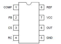
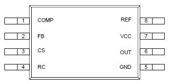
Same Pinout as UCC3802, UC3842, and UC3842APinout

PIN DESCRIPTIONS
COMP: COMP is the output of the error amplifier and the input of the PWM comparator.
Unlike other devices, the error amplifier in the UCC3813 family is a true, low output-impedance, 2MHz operational amplifier. As such, the COMP terminal can both source and sink current. However, the error amplifier is internally current limited, so that you can command zero duty cycle by externally forcing COMP to GND.
The UCC3813 family features built-in full cycle Soft Start.Soft Start is implemented as a clamp on the maximum COMP voltage.
FB: FB is the inverting input of the error amplifier. For best stability, keep FB lead length as short as possible and FB stray capacitance as small as possible.
CS: CS is the input to the current sense comparators.The UCC3813 family has two different current sense comparators: the PWM comparator and an over-current comparator.
The UCC3813 family contains digital current sense filtering,which disconnects the CS terminal from the current sense comparator during the 100ns interval immediately following the rising edge of the OUT pin. This digital filtering,also called leading-edge blanking, means that in most applications, no analog filtering (RC filter) is required on CS. Compared to an external RC filter technique,the leading-edge blanking provides a smaller effective CS to OUT propagation delay. Note, however,that the minimum non-zero On-Time of the OUT signal is directly affected by the leading-edge-blanking and the CS to OUT propagation delay.
The over-current comparator is only intended for fault sensing, and exceeding the over-current threshold will cause a soft start cycle.
RC: RC is the oscillator timing pin. For fixed frequency operation, set timing capacitor charging current by connecting a resistor from REF to RC. Set frequency by connecting a timing capacitor from RC to GND. For best performance, keep the timing capacitor lead to GND as short and direct as possible. If possible, use separate ground traces for the timing capacitor and all other functions.
GND: GND is reference ground and power ground for all functions on this part.
OUT: OUT is the output of a high-current power driver capable of driving the gate of a power MOSFET with peak currents exceeding ±750mA. OUT is actively held low when VCC is below the UVLO threshold.The high-current power driver consists of FET output devices,which can switch all of the way to GND and all of the way to VCC. The output stage also provides a very low impedance to overshoot and undershoot. This means that in many cases, external schottky clamp diodes are not required.
VCC: VCC is the power input connection for this device.In normal operation VCC is powered through a current limiting resistor. Although quiescent VCC current is verylow, total supply current will be higher, depending on OUT current. Total VCC current is the sum of quiescent VCC current and the average OUT current. Knowing the operating frequency and the MOSFET gate charge (Qg),average OUT current can be calculated from:
IOUT =Qg •F .
To prevent noise problems, bypass VCC to GND with a ceramic capacitor as close to the VCC pin as possible.An electrolytic capacitor may also be used in addition to the ceramic capacitor.
REF: REF is the voltage reference for the error amplifier and also for many other functions on the IC. REF is also used as the logic power supply for high speed switching logic on the IC.
When VCC is greater than 1V and less than the UVLO threshold, REF is pulled to ground through a 5kW resistor.This means that REF can be used as a logic output indicating power system status. It is important for reference stability that REF is bypassed to GND with a ceramic capacitor as close to the pin as possible. An electrolytic capacitor may also be used in addition to the ceramic capacitor. A minimum of 0.1F ceramic is required.Additional REF bypassing is required for external loads greater than 2.5mA on the reference.
To prevent noise problems with high speed switching transients, bypass REF to ground with a ceramic capacitor very close to the IC package.
SpecificationsVCC Voltage (Note 2) . . . . . . . . . . . . . . . . . .. . . . . . . . . 12.0V
VCC Current . . . . . . . . . . . . . . . . . . . . . . . . . . . . . . . . 30.0mA
OUT Current . . . . . . . . . . . . . . . . . . . . . . . . . . . . . . . . . . 1.0A
OUT Energy (Capacitive Load) . . . . . . . . . . . . . . . . . . . 20.0mJ
Analog Inputs (FB, CS) . . . . . . . . . . . . . . . . . .. . 0.3V to 6.3V
Power Dissipation at TA < +25°C (N Package). . . . . . . . 1.0W
Power Dissipation at TA < +25°C (D Package). . .. . . . . 0.65W
Storage Temperature . . . . . . . . . . . . .. . . . . 65 C to +150°C
Junction Temperature. . . . . . . . . . . . . . . . . . 55 C to +150°C
Lead Temperature (Soldering, 10 Seconds). . . . . . . . . +300°CDescriptionThe UCC3813-0/-1/-2/-3/-4/-5 family of high-speed, low-power integrated circuits contain all of the control and drive components required for off-line and DC-to-DC fixed frequency current-mode switching power supplies with minimal parts count.
These devices UCC3813-0/-1/-2/-3/-4/-5 have the same pin configuration as the UC3842/3/4/5 family, and also offer the added features of internal full-cycle soft start and internal leading-edge blanking of the current-sense input.

 UCC2813-0 Data Sheet

