UCC27221

Features: · Maximizes Efficiency by Minimizing Body-Diode Conduction and Reverse Recovery Losses· Transparent Synchronous Buck Gate Drive Operation From the Single Ended PWM Input Signal· 12-V or 5-V Input Operation· 3.3-V Input Operation With Availability of 12-V Bus Bias· On-Board 6.5-V Gate Dri...

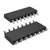
product image

UCC27221 Picture
SeekIC No. : 004535814 Detail

UCC27221: Features: · Maximizes Efficiency by Minimizing Body-Diode Conduction and Reverse Recovery Losses· Transparent Synchronous Buck Gate Drive Operation From the Single Ended PWM Input Signal· 12-V or 5-...

floor Price/Ceiling Price

Part Number:
UCC27221
Supply Ability:
5000

Price Break

  • Qty
  • 1~5000
  • Unit Price
  • Negotiable
  • Processing time
  • 15 Days
Total Cost: $ 0.00

SeekIC Buyer Protection PLUS - newly updated for 2013!

  • Escrow Protection.
  • Guaranteed refunds.
  • Secure payments.
  • Learn more >>

Month Sales

268 Transactions

Rating

evaluate  (4.8 stars)

Upload time: 2025/1/7

Payment Methods

All payment methods are secure and covered by SeekIC Buyer Protection PLUS.

Notice: When you place an order, your payment is made to SeekIC and not to your seller. SeekIC only pays the seller after confirming you have received your order. We will also never share your payment details with your seller.
Product Details

Description


Features:

· Maximizes Efficiency by Minimizing Body-Diode Conduction and Reverse Recovery Losses
· Transparent Synchronous Buck Gate Drive Operation From the Single Ended PWM Input Signal
· 12-V or 5-V Input Operation
· 3.3-V Input Operation With Availability of 12-V Bus Bias
· On-Board 6.5-V Gate Drive Regulator
· ±3.3-A TrueDrive™Gate Drives for High Current Delivery at MOSFET Miller Thresholds
· Automatically Adjusts for Changing Operating Conditions
· Thermally Enhanced 14-Pin PowerPAD™
    HTSSOP Package Minimizes Board Area and Junction Temperature Rise


Application

· Non-Isolated Single or Multi-phased DC-to-DC Converters for Processor Power, General Computer, Telecom and Datacom Applications


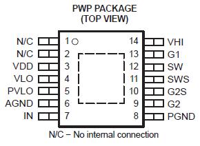
Pinout

  Connection Diagram


Specifications

Supply voltage range, VDD . . . . . . . . . . . . . . . . . . . . . . . . . . . . . . −0.3 to 20 V
Input voltage, VHI . . . . . . . . . . . . . . . . . . . . . . . . . . . . . . . . . . . . . . . . . . . 30 V
SW, SWS . . . . . . . . . . . . . . . . . . . . . . . . . . . . . . . . . . . . . . . . . . . . . . . . . . 20 V
Supply current, IDD, including gate drive current . . . . . . . . . .  . . . . . . .100 mA
Sink current (peak) pulsed, G1/G2 . . . . . . . . . . . . . . . . . . . . . . . . . . . . . . 4.0 A
Source current (peak) pulsed, G1/G2 . . . . . . . . . . . . . . . . . . . . . . . . . . . −4.0 A
Analog input, IN . . . . . . . . . . . . . .  . −3.0 V to VDD + 0.3 V, not to exceed 15 V
Power Dissipation at TA = 25°C (PWP package) . . . . . . . . . . . . . . . . . . . . 3 W
Operating junction temperature range, TJ . . . . . . . . . . . . . . −55°C to 115°C
Storage temperature range, Tstg . . . . . . . . . . . . . . . . . . . . . −65°C to 150°C
Lead temperature soldering 1.6 mm (1/16 inch)
from case for 10 seconds . . .  . . . .................................................... . . 300°C

† Stresses beyond those listed under "absolute maximum ratings" may cause permanent damage to the device. These are stress ratings only, and functional operation of the device at these or any other conditions beyond those indicated under "recommended operating conditions" is not implied. Exposure to absolute-maximum-rated conditions for extended periods may affect device reliability.
‡ All voltages are with respect to AGND and PGND. Currents are positive into, negative out of the specified terminal.


Description

The UCC27221 and UCC27222 are high-speed synchronous buck drivers for today's high-efficiency, lower-output voltage designs. Using Predictive Gate Drive™  (PGD) control technology, these drivers reduce diode conduction and reverse recovery losses in the synchronous rectifier MOSFET(s). The UCC27221 has an inverted PWM input while the UCC27222 has a non-inverting PWM input.

Predictive Gate Drive ™ technology uses controlloops which are stabilized internally and are therefore transparent to the user. These loops use no external components, so no additional design is needed to take advantage of the higher efficiency of these drivers.

This closed loop feedback system detects body-diode conduction, and adjusts deadtime delays to minimize the conduction time interval. This virtually eliminates body-diode conduction while adjusting for temperature, load- dependent delays, and for different MOSFETs. Precise gate timing at the nanosecond level reduces the reverse recovery time of the synchronous rectifier MOSFET body-diode, reducing reverse recovery losses seen in the main (high-side) MOSFET. The lower junction temperature in the low-side MOSFET increases product reliability. Since the power dissipation is minimized, a higher switching frequency can also be used, allowing for smaller component sizes.

The UCC27221 and UCC27222 are offered in the thermally enhanced 14-pin PowerPAD™ package with 2°C/W jc.


Customers Who Bought This Item Also Bought

Margin,quality,low-cost products with low minimum orders. Secure your online payments with SeekIC Buyer Protection.
Potentiometers, Variable Resistors
Batteries, Chargers, Holders
Audio Products
Memory Cards, Modules
Semiconductor Modules
Boxes, Enclosures, Racks
View more