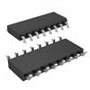
Features: ` Specified from -40 to 140 ` Drives Two N-Channel MOSFETs in High-Side/Low-Side Configuration` Maximum Boot Voltage 120 V` Maximum VDD Voltage 20 V` On-Chip 0.65-V VF, 0.6-W RD Bootstrap Diode` Greater than 1 MHz of Operation` 20-ns Propagation Delay Times` 3-A Sink, 3-A Source Output ...
UCC27200: Features: ` Specified from -40 to 140 ` Drives Two N-Channel MOSFETs in High-Side/Low-Side Configuration` Maximum Boot Voltage 120 V` Maximum VDD Voltage 20 V` On-Chip 0.65-V VF, 0.6-W RD Bootstrap...
SeekIC Buyer Protection PLUS - newly updated for 2013!
268 Transactions
All payment methods are secure and covered by SeekIC Buyer Protection PLUS.
PARAMETER | VALUE | UNIT | |
Supply voltage range, (2) VDD | -0.3 to 20 | V | |
Input voltages on LI and HI, VLI, VHI | -0.3 to 20 | ||
Output voltage on LO, VLO | DC | -0.3 to VDD + 0.3, | |
Repetitive pulse <100 ns | -2 to VDD + 0.3 | ||
Output voltage on HO, VHO | DC | VHS 0.3 to VHB + 0.3 | |
Repetitive pulse <100 ns | VHS - 2 to VHB + 0.3, (VHB - VHS <20) | ||
Voltage on HS, VHS | DC | -1 to 120 | |
Repetitive pulse <100 ns | -5 to 120 | ||
Voltage on HB, VHB | -0.3 to 120 | ||
Voltage On HB-HS | -0.3 to 20 | ||
Operating virtual junction temperature range, TJ | -40 to +150 | ||
Storage temperature, TSTG | -65 to +150 | ||
Lead temperature (soldering, 10 sec.) | +300 | ||
Power dissipation at TA = 25 (D package) (3) | 1.3 | W | |
Power dissipation at TA = 25 (DDA package)(3) | 2.7 | ||
Power dissipation at TA = 25 (DRM package) (3) | 3.3 |
(1) Stresses beyond those listed under "absolute maximum ratings" may cause permanent damage to the device. These are stress ratings only, and functional operation of the device at these or any other conditions beyond those indicated under "recommended operating conditions" is not implied. Exposure to absolute-maximum-rated conditions for extended periods may affect device reliability.
(2) All voltages are with respect to Vss. Currents are positive into, negative out of the specified terminal.
(3) This data was taken using the JEDEC proposed high-K test PCB. See THERMAL CHARACTERISTICS section for details.
The UCC27200/1 family of high frequency N-Channel MOSFET drivers include a 120-V bootstrap diode and high-side/low-side driver with independent inputs for maximum control flexibility. This allows for N-Channel MOSFET control in half-bridge, full-bridge, two-switch forward and active clamp forward converters. The low-side and the high-side gate drivers are independently controlled and matched to 1-ns between the turn-on and turn-off of each other.
An on-chip bootstrap diode eliminates the external discrete diodes. Under-voltage lockout is provided for both the high-side and the low-side drivers forcing the outputs low if the drive voltage is below the specified threshold.
Two versions of the UCC27200 are offered. The UCC27200 has high noise immune CMOS input thresholds while the UCC27201 has TTL compatible thresholds.
Both devices UCC27200/1 are offered in 8-pin SOIC (D), PowerPad™ SOIC-8 (DDA) and SON-8 (DRM) packages.