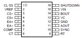
Features: · Pin-for-Pin Compatible With the UC2846
· 65-ns Typical Delay From Shutdown to Outputs and 50-ns Typical Delay From Sync to Outputs
· Improved Current Sense Amplifier With Reduced Noise Sensitivity
· Differential Current Sense With 3-V Common Mode Range
· Trimmed Oscillator Discharge Current for Accurate Deadband Control
· Accurate 1-V Shutdown Threshold
· High Current Dual Totem Pole Outputs (1.5-A peak)
· TTL Compatible Oscillator SYNC Pin Thresholds
· 4-kV ESD ProtectionPinout Specificationsover operating free-air temperature range (unless otherwise noted)(1) (2)
| |
UNIT |
| Supply voltage |
40 V |
| Collector supply voltage |
40 V |
| IO Output current (sink or source) |
DC |
0.5 A |
| Pulse (0.5 ms) |
2 A |
| Error amplifier input voltage |
0.3 V to VIN |
| Shutdown input voltage |
0.3 V to 10 V |
| Current sense input voltage |
0.3 V to 3 V |
| SYNC output current |
±10 mA |
| Error amplifier output current |
-5 mA |
| Soft start sink current |
50 mA |
| Oscillator charging current |
5 mA |
| Power dissipation |
TA = 25°C |
1 W |
| TC = 25°C |
2 W |
| TJ Operating junction temperature range |
55°C to 150°C |
| Tstg Storage temperature range |
65°C to 150°C |
| Lead temperature soldering 1,6 mm (1/16 inch) from case for 10 seconds |
300°C |
(1) Stresses beyond those listed under "absolute maximum ratings" may cause permanent damage to the device. These are stress ratings only, and functional operation of the device at these or any other conditions beyond those indicated under "recommended operating conditions" is not implied. Exposure to absolute-maximum-rated conditions for extended periods may affect device reliability.
(2) Unless otherwise indicated, voltages are reference to ground and currents are positive into and negative out of the specified terminals.
DescriptionThe UC2856 is a high performance version of the popular UC2846 series of current mode controllers, and is intended for both design upgrades and new applications where speed and accuracy are important. All input to output delays have been minimized, and the current sense output is slew rate limited to reduce noise sensitivity. Fast 1.5-A peak output stages have been added to allow rapid switching of power FETs.
A low impedance TTL compatible sync output has been implemented with a 3-state function when used as a sync input.
Internal chip grounding has been improved to minimize internal noise caused when driving large capacitive loads. This, in conjunction with the improved differential current sense amplifier, results in enhanced noise immunity.
Other features include a trimmed oscillator current (8%) for accurate frequency and dead time control; a 1 V, 5% shutdown threshold; and 4 kV minimum ESD protection on all pins.

 UC2856Q Data Sheet


