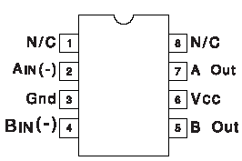
Features: · 25ns Rise and Fall into 1000pF· 15ns Propagation Delay· 1.5A Source or Sink Output Drive· Operation with 5V to 35V Supply· High-Speed Schottky NPN Process· 8-PIN MINIDIP PackagePinoutSpecificationsInput Supply Voltage, VCC. . . . . . . . . . . . . . . . . . . . . .. . . . 40VOutput Cur...
UC1711: Features: · 25ns Rise and Fall into 1000pF· 15ns Propagation Delay· 1.5A Source or Sink Output Drive· Operation with 5V to 35V Supply· High-Speed Schottky NPN Process· 8-PIN MINIDIP PackagePinoutSpe...
SeekIC Buyer Protection PLUS - newly updated for 2013!
268 Transactions
All payment methods are secure and covered by SeekIC Buyer Protection PLUS.
Input Supply Voltage, VCC. . . . . . . . . . . . . . . . . . . . . .. . . . 40V
Output Current (Source or Sink)
Steady State . . . . . . . . . . . . . . . . . . . . . . . . . . . . . ± 500mA
Peak Transient . . . . . . . . . . . . . . . . . . . . . . . . . . . . . ± 1.5A
Maximum Forced Voltage . . . . . . . . . . . . . . . . . . . .. -0.3V to 7V
Maximum Forced Current . . . . . . . . . . . . . . . . . . . . . . . ± 10mA
Power Dissipation . . . . . . . . . . . . . . . . . . . . . . . . . . . . . . . . 1W
Operating Junction Temperature . . . . . . . . .. . 55 to +150
Storage Temperature . . . . . . . . . . . . . . . . . . . 65 to +150
Note 1: Unless otherwise indicated, voltages are reference to ground and currents are positive into, negative out
of, the specified terminals. All reliability information for this device has been gathered at an ambient
air temperature of 125, and a supply voltage of 25V.
Note 2: Consult Unitrode databook for information regarding thermal specifications and limitations of packages.
The UC1711 family of FET drivers are made with an all-NPN Schottky process in order to optimize switching speed, temperature stability, and radiation resistance. The cost for these benefits is a quiescent supply current which varies with both output state and supply voltage. For lower power requirements, refer to the the UC1709 family which is both pin compatible with, and functionally equivalent to the UC1711.
These devices UC1711 implement inverting logic with TTL compatible inputs, and output stages which will either source, or sink in excess of 1.5A of load current with minimal cross-conduction charge. Due to their monolithic construction, the channels are well matched and can be paralleled for doubled output current capability.